Hello Everyone!
I have designed (okay okay, copied ) a current mode PSU with UCC2808 IC, from Texas. I read all the available documents (how works the current mode, current mode VS. volate mode, etcetcetc).
On the UCC2808 IC's datasheet, there's a DC/DC converter for 5V@10Amps.
I modified a little bit that circuit, to produce 2x50V @ 3A. I did this by changing the resistors neard the TL431, for higher voltage. And for the higher current limit, I changed the voltage divider near the current sense resistor. I reduced 2.8k.
But... When there's no load (just 2 1k soldered under the ouptut capacitors) the output voltage is OK. The feedback is taken from only 50V, not from 2x50V. Oh, and the "50V" is not really 50V, it's 54V, becouse I don't have 1% resistors, and I wouldn't like to use trim.pot.
When I load the regulated 54V with 100ohm, then the voltage is fine, about 54V. But when I change the load from 100ohm to 16ohm, the voltage drops to 40V. Why?
And another thing.
Sometimes the PSU is oscillating. I can hear it from the transformer (ETD49). Maybe, should I solder some bigger capacitor near the TL431, to slow down the feedback?
I attached the original schematic.
I have designed (okay okay, copied
) a current mode PSU with UCC2808 IC, from Texas. I read all the available documents (how works the current mode, current mode VS. volate mode, etcetcetc). On the UCC2808 IC's datasheet, there's a DC/DC converter for 5V@10Amps.
I modified a little bit that circuit, to produce 2x50V @ 3A. I did this by changing the resistors neard the TL431, for higher voltage. And for the higher current limit, I changed the voltage divider near the current sense resistor. I reduced 2.8k.
But... When there's no load (just 2 1k soldered under the ouptut capacitors) the output voltage is OK. The feedback is taken from only 50V, not from 2x50V. Oh, and the "50V" is not really 50V, it's 54V, becouse I don't have 1% resistors, and I wouldn't like to use trim.pot.
When I load the regulated 54V with 100ohm, then the voltage is fine, about 54V. But when I change the load from 100ohm to 16ohm, the voltage drops to 40V. Why?
And another thing.
Sometimes the PSU is oscillating. I can hear it from the transformer (ETD49). Maybe, should I solder some bigger capacitor near the TL431, to slow down the feedback?
I attached the original schematic.
Attachments
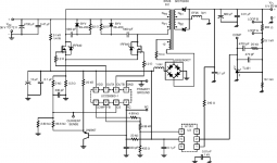
Here is my schematic. You can see how is regulated the output. The difference between the regulated & unreg. output is only a few volts.
Unfortunatelly, this kind of secondary-arrangement, and rectifying is not good I realised it, while I was winding the transformer.
The transformer's window area isn't optimally utilized, becouse of that 4 secondary windings.
Unfortunatelly, this kind of secondary-arrangement, and rectifying is not good
I realised it, while I was winding the transformer. The transformer's window area isn't optimally utilized, becouse of that 4 secondary windings.
Attachments
Noise coupling to current sense or feedback? check controller ic all pins for abnormal waveforms or spikes, especially current sense.Danko said:Hello Everyone!
When I load the regulated 54V with 100ohm, then the voltage is fine, about 54V. But when I change the load from 100ohm to 16ohm, the voltage drops to 40V. Why?
.
How is your board layout look like, it can have bigger importance than actual schematic and component values.
Voltage Drop
Danko-
Schematically, your circuit looks good. However, how are things we can not see? Like the transformer core size? The wire size? and the MOSFET capacity? What is your input voltage? Is it still the 36-72V as called for in the original Texas Instruments schematic, or is it +12V?
Also, try changing the current sense resistor to a MUCH lower value, like 0.01Ohm. This is because at a 30A draw from the primary side (at full power output), your 0.22 Ohm resistors will develop something like (30A x 0.22 Ohm) = 6.6V at the UCC2808's current sense pin. As I recall, the current-limit threshhold at this pin is 1.0V. A 0.01 Ohm resistor will develop only 300mV across this resistor, and with the current spikes from each cycle, this will just about approach (but not exceed) the '2808's current-sense threshhold. TI should have a good tutorial for calculating the value of the current-sense resistor.
Also, I realize the IRF540s are very robust MOSFETs, but you might try paralleling them, 2 per side of the primary. This will let them run much cooler at full load with considerably less stress and provide a backup if one MOSFET should fail.
Or better yet, you could try a MOSFET with much lower Rds(on). like the MTP75N06E from OnSemi. This is a 60V, 75A unit with an Rds(on) of only 0.010 Ohms (ten milli-ohms), while the IRF540 is 0.077 Ohms. This is a seven-fold reduction on Power Dissipation for conduction losses.
Hope these tips help. Let me know how these tips work out.
Regards,
Steve
Danko-
Schematically, your circuit looks good. However, how are things we can not see? Like the transformer core size? The wire size? and the MOSFET capacity? What is your input voltage? Is it still the 36-72V as called for in the original Texas Instruments schematic, or is it +12V?
Also, try changing the current sense resistor to a MUCH lower value, like 0.01Ohm. This is because at a 30A draw from the primary side (at full power output), your 0.22 Ohm resistors will develop something like (30A x 0.22 Ohm) = 6.6V at the UCC2808's current sense pin. As I recall, the current-limit threshhold at this pin is 1.0V. A 0.01 Ohm resistor will develop only 300mV across this resistor, and with the current spikes from each cycle, this will just about approach (but not exceed) the '2808's current-sense threshhold. TI should have a good tutorial for calculating the value of the current-sense resistor.
Also, I realize the IRF540s are very robust MOSFETs, but you might try paralleling them, 2 per side of the primary. This will let them run much cooler
at full load with considerably less stress and provide a backup if one MOSFET should fail.Or better yet, you could try a MOSFET with much lower Rds(on). like the MTP75N06E from OnSemi. This is a 60V, 75A unit with an Rds(on) of only 0.010 Ohms (ten milli-ohms), while the IRF540 is 0.077 Ohms. This is a seven-fold reduction on Power Dissipation
for conduction losses. Hope these tips help. Let me know how these tips work out.
Regards,
Steve
I've attached the board layout.
The Q1 Q2 are the FETs. They are IRF540N. RDS_on=44mOhm, max. Current is 33Amper. They are mounted on the component side of the PCB, and that big place is used az a heatsink. The another 2 TO22 package are the two diodes. FEP16JT from Vishay. They are mounted the same way, as the FETs. U$5 is the output choke. The transformer is an ETD49. The primary winding is 2x6 turns. The secondary is 4x15 windings. I paralelled 0.4mm diameter CuZ copper wires. 12 paralelled wires in the primer, and /AFAIK/ 6 paralelled wires in the secondary.
This "stuff" is only a testing-circuit, to learn how current mode works, what are the basics, etcetcetc. I'm "in switched mode" for about 1 year. Under this time, I read a loooot of docs, made a few buck regulators, boost-converters.
In this circuit I can play /almost/ without risking my life, and my wallet, with burning expensive 500V/20A MOSFETs
Thank you for you patience!
Attachments
Danko said:The transformer is an ETD49. The primary winding is 2x6 turns. The secondary is 4x15 windings. I paralelled 0.4mm diameter CuZ copper wires. 12 paralelled wires in the primer, and /AFAIK/ 6 paralelled wires in the secondary.
The frequency is about 140kHz.
The ouput choke: 2x40-45 turns on an Al=200 iron powder core.
The maximum induction of that iron powder core is about 780AmperTurns. The output capacitors are 2x1000uF paralelled with 1-1uF WIMA foil capacitors. Unfortunatelly they /the 1000uF/ are not LOW-ESR type, but the foil-capacitors have very low ESR.
I know, that a single center-tapped secondary winding would have done the job for symmetrical output, but haven't got any common anode double-diode at home
Using 4 diodes would infrease the PCB area.
In the next version PCB i'm going to figure out somethin else, becouse this arrangement of secondary winding wastes a lot of space on the transformer.
Danko said:Danko said:The transformer is an ETD49. The primary winding is 2x6 turns. The secondary is 4x15 windings. I paralelled 0.4mm diameter CuZ copper wires. 12 paralelled wires in the primer, and /AFAIK/ 6 paralelled wires in the secondary.
The frequency is about 140kHz.
The ouput choke: 2x40-45 turns on an Al=200 iron powder core.
The maximum induction of that iron powder core is about 780AmperTurns. The output capacitors are 2x1000uF paralelled with 1-1uF WIMA foil capacitors. Unfortunatelly they /the 1000uF/ are not LOW-ESR type, but the foil-capacitors have very low ESR.
I know, that a single center-tapped secondary winding would have done the job for symmetrical output, but haven't got any common anode double-diode at home
Using 4 diodes would infrease the PCB area.
In the next version PCB i'm going to figure out somethin else, becouse this arrangement of secondary winding wastes a lot of space on the transformer.
Have you checked waveforms? (and use short ground-lead for scope probe)
CS pin might reveal something on this problem
Well, with : 50V in, 54V out and 6:15 trafo, the converter is going to reflect 125V to each secondary winding and to operate at approx 44% steady state duty cycle when in continuous conduction (200V output diodes required).
With 280khz oscillator, 125V reflected to the secondary, 54V output and 44% duty cycle, we would get 0.34A p-p current ripple in each 320uH buck inductor. Should the inductance value decrease with increased current, ripple would also increase proportionally.
Loading one of the outputs with 16 ohms, output current is going to be 3.38A, adding half of the inductor ripple we would get 3.54A peak, that would translate into 8.86A reflected to the primary side.
8.86A is going to produce 2V voltage drop across your 0.22 ohm current sense resistor. Taking into consideration the 2k/2.8k attenuator, and neglecting the effect of slope compensation, 1.17V peak would be applied to the CS pin of UCC2808.
However, CS input signal is specified to be between 0 and 500mV for normal operation, and overcurrent protection is triggered somewhere between 700 and 800mV.
Furthermore, if we take 40V output and 16 ohm load and calculate the peak voltage applied to CS pin in these circumstances, we get 0.84V. It's just above the current limiting threshold, so current limiting is taking place.
You should redesign the circuit to use a current limit consistent with your maximum expected load.
I think, I solved the PSU-oscillating-problem. I connected the primary side, and the sedondary side GND with a 100nF capacitor paralelled with 1MOhm resistor. After this sometimes the PSU oscillated, but I soldered some capacitors near the TL431.
Eva: Thanks a lot! I will do some calculations about the surrent-sense resistor.
I decreased the frequency about half of 280kHz. How did you calculate the current ripple in the output inductor?
Why is required the slope compensation in push-pull topology? I read, that slope-compensation is required only when the duty-cycle is higher (or will be...) higher than 50%. But in push-pull applications, the duty-cycle can be maximum 50%, becouse of the simmetry. If we take into consideration the dead-time, then the max. duty-cycle can be about 45-47%.
Why is there a slope-compensation in the original schematic?
Regarding the current-sense resistor ....
So, I have to calculate the values, to get about 700mV on the CS pin at maximum output power?
Danko said:I think, I solved the PSU-oscillating-problem. I connected the primary side, and the sedondary side GND with a 100nF capacitor paralelled with 1MOhm resistor. After this sometimes the PSU oscillated, but I soldered some capacitors near the TL431.
This capacitor, placed directly across transformer pins, definitely reduces common mode EMI, but usual values are somewhat smaller than 100nF. Most off-line SMPS units use a 4.7nF 2KV capacitor and it's enough to force common-mode current due to switching transients and primary-secondary capacitance to flow back through the capacitor.
Danko said:Eva: Thanks a lot! I will do some calculations about the surrent-sense resistor.
I decreased the frequency about half of 280kHz. How did you calculate the current ripple in the output inductor?
When you apply a constant voltage 'V' to a inductor of 'L' henries during a time of 't' seconds you get a linear current ramp whose slope in volts/second is V/L. Multiply that slope by the time it lasts and you'll get peak to peak current ripple.
For example :
V = Vreflected-Vout-Vdiode = 125-54-1 = 70V
L = 320uH
duty_cycle= (Vout+Vdiode)/Vreflected = (55+1)/125 = 44%
osc_freq=280Khz
t = duty_cycle/osc_freq = .44/280,000 = 1.57uS
Iripple= 70V * 1.57uS / 320uH = 0.34A p-p
The inductor dicharge period may be also used:
V = Vout+Vdiode = 54+1 = 55V
L = 320uH
duty_cycle=44% so discharge time is 56%
osc_freq=280Khz
t = .56/280,000 = 2us
Iripple= 55V * 2uS / 320uH = 0.34A p-p
An usual rule of thumb is to allow current ripple to be up to 20% of the maximum output current, so you may decrease the operating frequency if you transformer allows for it. Note that 140/280Khz are insane frequencies from the switching-losses point of view and that your transformer may allow even 40/80Hz operation.
Danko said:Why is required the slope compensation in push-pull topology? I read, that slope-compensation is required only when the duty-cycle is higher (or will be...) higher than 50%. But in push-pull applications, the duty-cycle can be maximum 50%, becouse of the simmetry. If we take into consideration the dead-time, then the max. duty-cycle can be about 45-47%.
Why is there a slope-compensation in the original schematic?
As seen from the current-mode control loop point of view, the transformer and the push-pull action does not exist at all and operating frequency is Fosc instead of Fosc/2, so duty cycles in push pull may also approach 100%. That's why slope compensation is also required.
But note that you are using a 15:6 transformer to get only 50V output from 50V input and this means that steady state duty cycle may hardly reach 50%, so slope compensation may not be required in these circumstances. However, this 15:6 ratio also means that current flowing through the primary side is more than twice the sum of output currents and this fact is going to hurt efficiency very badly. I would use a lower ratio like 6:8 or 6:10 instead, even at the expense of having to mess with slope compensation.
Danko said:Regarding the current-sense resistor ....
So, I have to calculate the values, to get about 700mV on the CS pin at maximum output power?
Right, but the datasheet recommends a 0 to 500mV range for normal operation, so I would design for 500mV instead.
Thank you, Eva!
If I know the I_rippe, how can I calculate the Voltage_ripple?
U_ripple = outputcapacitor's-ESR * I_ripple?
This is the new layout:
http://sziget.mine.nu/~danko/aramkor/Screenshot-181.jpg
The box with green lines is the toroid output choke. Are the trafo and the output choke on good position? Or will they interfere each other's magnetic field?
If I don't need slope compensation, then can I omit the T1 transistor from the CIRCUIT ?
Why is bad, if I put 100nF instead of the 4.7nF/2kV capacitor?
Thanks in advance!
Danko said:Thank you, Eva!
If I know the I_rippe, how can I calculate the Voltage_ripple?
U_ripple = outputcapacitor's-ESR * I_ripple?
This is not so simple. Use your favorite circuit simulator to check how capacitor voltage waveform looks when a current triangle wave with the same parameters as the inductor ripple current is flowing through them. Remember to model output capacitors with some ESR and maybe a slightly bit of ESL in series.
Danko said:
This is the new layout:
http://sziget.mine.nu/~danko/aramkor/Screenshot-181.jpg
The box with green lines is the toroid output choke. Are the trafo and the output choke on good position? Or will they interfere each
other's magnetic field?
Both an ungapped transformer and a toroid inducor are not going to generate strong stray magnetic fields. Also, they are hardly going to intererfere between them. Anyway, the inductor is conveniently placed away from the control circuit (this is usually more critical).
Danko said:
With your 6+6:15+15 turn ratio slope compensation is hardly required, altough there are a lot of reasons to use it anyway. I recommend reading that paper carefully:
http://www.powerdesigners.com/InfoWeb/design_center/Appnotes_Archive/u97.pdf
Furthermore, being able to use duty cycles above 50% will allow for a more performance-wise primary to secondary turn ratio in the transformer, thus reducing primary side currents by approx. 40%, and reducing both inductor current ripple and output voltage ripple due to the increased duty cycle.
Danko said:
Why is bad, if I put 100nF instead of the 4.7nF/2kV capacitor?
Thanks in advance!
It causes much more AC leakage between primary and secondary than required and hurts isolation, otherwise it's fine.
Finally!! My SMPS is working /almost)/ perfect!!
I put an amplifier at the output of my SMPS, and there's no noise on the amp's output)
How "flat" should the ouput of the SMPS have to be? The output is 2x40V, and there are small spikes, about 200mV "high". Is it OK?
Could someone take a photo of a home-made SMPS's output?
)/ perfect!!I put an amplifier at the output of my SMPS, and there's no noise on the amp's output
) How "flat" should the ouput of the SMPS have to be? The output is 2x40V, and there are small spikes, about 200mV "high". Is it OK?
Could someone take a photo of a home-made SMPS's output?
Danko:
I'm glad to hear your SMPS is working well now.
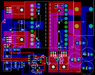
I just have a personal comment, for what it's worth, on your PCB layout.
Why are the copper lands on the MOSFET Drains so large? They are much larger than current capacity would dictate them to be (about 5 mm).
"Noisy" nodes should never be given large copper areas, and this is the noisiest node in the circuit. The MOSFET Source, lifted above ground by the current sense R, is also not the quietest node around either. I would expect these two nodes to be small, short traces, well covered with ground plane on the top layer (which is conspicuously absent in your layout). I frankly don't like 2-sided PCB's for such simple circuits, because of the extra work, but if I must use double sided, then it's imperative that I paint ground plane everywhere I can. The main reason to use 2-sided in SMPS is NOT to make it easier to route your wires. It's to provide ground plane.
I see you have shortened your gate drive nodes from a previous layout--that stood out like a sore thumb initially. Wise move.
Adrian
I'm glad to hear your SMPS is working well now.
I just have a personal comment, for what it's worth, on your PCB layout.
Why are the copper lands on the MOSFET Drains so large? They are much larger than current capacity would dictate them to be (about 5 mm).
"Noisy" nodes should never be given large copper areas, and this is the noisiest node in the circuit. The MOSFET Source, lifted above ground by the current sense R, is also not the quietest node around either. I would expect these two nodes to be small, short traces, well covered with ground plane on the top layer (which is conspicuously absent in your layout). I frankly don't like 2-sided PCB's for such simple circuits, because of the extra work, but if I must use double sided, then it's imperative that I paint ground plane everywhere I can. The main reason to use 2-sided in SMPS is NOT to make it easier to route your wires. It's to provide ground plane.
I see you have shortened your gate drive nodes from a previous layout--that stood out like a sore thumb initially. Wise move.
Adrian
- Status
- This old topic is closed. If you want to reopen this topic, contact a moderator using the "Report Post" button.
- Home
- Amplifiers
- Power Supplies
- UCC208 current mode IC usage help NEEDED