Hello people.
This is my first PCB/PSU/gainclone-related design ever.
I do understand it is lame, however - I would like to ask you to take a look at it and provide me with some feedback. This is going to power two LM3875's. I am going to etch it myself, and this is only for my very first prototype.
Thanks!")
This is my first PCB/PSU/gainclone-related design ever.
I do understand it is lame, however - I would like to ask you to take a look at it and provide me with some feedback. This is going to power two LM3875's. I am going to etch it myself, and this is only for my very first prototype.
Thanks!
Attachments
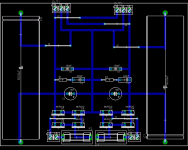
Use more thicker foils on the GND, the positive and the negative rails. You are making a very big panel, so, you can use very very thick foils. Your panel will be good, when you see more blue on the picture, than black
It is electrically good, and it es environment-friendly, becouse of the low amount of copper, to be removed.
Put under each 5000uF capacitors one-one 100nF/ceamic capacitors, for high-frequenzy bypassing, and put C6 C5 closer to C1 C2.
If I were you, I would do theese changes
It is electrically good, and it es environment-friendly, becouse of the low amount of copper, to be removed.
Put under each 5000uF capacitors one-one 100nF/ceamic capacitors, for high-frequenzy bypassing, and put C6 C5 closer to C1 C2.
If I were you, I would do theese changes
Hi,
I think you should double or triple the width of your hi current tracks.
Try to minimise the length of the tracks from caps to output to lower the inductance. There is room to squeeze everything in towards the middle & leave room for two more main caps.
How much power are your two gainclones going to produce?
2*5mF seems a tad light.
I see you plan to take a power ground to each gainclone. Now back track to where they meet in the top centre of your board. Now treat this as your central star ground. ALL your grounds must be referenced to a theroetical point here. A theoretical point is impossible so settle for a bolt through this central point and connect all the grounds to the board side of this bolted connection, not the copper side. That way the PSU pulse currents stay on the copper tracks and do not contaminate the clean side.
Connections to the central star ground include signal grounds for each channel, speaker returns, thiel networks (if any), mains earth (via a 10R//100nF or direct), on board decoupling and power grounds
Sorry if this is a bit long for a newcommer. Have a read & feel free to ask if anything needs further explanation.
Ditto. Much, much wider. If you are going to etch it yourself, the etching process will be quicker if there is less metal to remove. In fact, for an unregulated PS, I take a plain copper clad PCB, mark where the copper IS NOT and scribe/grind it away with a Demel tool. Ugly but fast, simple and effective.
Double sided is really not necessary for something like this. Especially, if you are going to etch your own, double sided can have some petty but annoying complications.
Double sided is really not necessary for something like this. Especially, if you are going to etch your own, double sided can have some petty but annoying complications.
Hi
I didnt quite understand the star ground suggestment.
Do you suggest I drop the two ground points and repalce them with a single 'terminal', to which I will connect all my ground signals?
It might be a bit of a problem finding a big enough screw-in terminal to hold all cables. Perhaps I can keep it this way and put another terminal in the center for signal/speaker return gound point while keeping the two other terminals?
Also, I plan on running two gaincloses, at about 30V for 8 ohm speakers.
If I try to make the width of the copper tracks bigger, the area of the rectifiers/wire conntectors on top becomes really crowded and i'm afraid that keeping only a small distance between tracks is not such a wise idea. What do you suggest (the current track width seemed to be a rather good compromise to me)?
Is there any nice way to avoid the entire (ugly) top part of the board while still allowing a convinient way to connect the power wires to the two amplifier modules?
Thanks again and again. You have no idea how much I appritiate your help.
Hi,
do not combine the two grounds to the power amps keep them separate right back to the star ground.
However I would not use a screw terminal for your grounds. You would then be relying on the one small soldered connection through the pin into the PCB. I really meant a bolt (brass or copper set screw about 3mm or 4mm diam) with nuts etc. You can then fit crimp connectors to each ground wire & bolt them all together.
Which part or parts do you need clarification on?
the main smoothing caps will see a peak current into 8 ohms of about 6A from the two gain clones. 8ohm speakers will have an impedance below nominal in, usually, 2 narrow frequency ranges. Into 6ohms about 8Apk current.
These are big currents for 5000uF (=5mF). I would try to fit double capacitors into your board space. It has the advantage of sharing the ripple current which can overheat your caps and seriously shorten their life, keep them cool and use 2 or even 3 in parallel.
sam9 said:Ditto. Much, much wider. If you are going to etch it yourself, the etching process will be quicker if there is less metal to remove. In fact, for an unregulated PS, I take a plain copper clad PCB, mark where the copper IS NOT and scribe/grind it away with a Demel tool. Ugly but fast, simple and effective.
Double sided is really not necessary for something like this. Especially, if you are going to etch your own, double sided can have some petty but annoying complications.
If your program allows it, lay a separate "net" as a ground plane. For my power supplies I specify the spacing of this net as 30 mils -- keeps tracks at least 30 mills away from adjacent tracks. You can physically connect this net at the ground plane. In many schematic capture programs the ground is specified as "Net 0". If you lay the ground plane with "Net 0" you are going to void the advantages of star grounding, (star grounding prevents current from waddling across the circuit board where you don't want it.) Of course, this plane also reduces the amount of copper you have to etch away.
EDIT: you may have a function to "remove islands", and "chamfer corners" -- these are also useful. After the ground plane is put down there are stranded "islands" which can be problematic. In ultiboard you just enable the island removal tool.

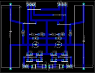
Another version. A bit ugly and seems like its gonna be the latest version for this prototype.
An externally hosted image should be here but it was not working when we last tested it.
Hi,
I preferred your original layout. Can you revert and upgrade that instead?
You still have a lot of empty board space in the middle. Can you rearrange the components to allow everything to fit a smaller board? But keep the wide tracks for the Hi current routes.
If you must keep the new layout you must sort the ground output area. All your charging pulses between the caps and rectifiers are passing through your ground reference.
Hi,
which part do you not understand?
Which terminal pins are too close together?
In your latest layout all the charging currents pass from the caps along to the T junction & then down to the rectifiers.
The very large currents on this route generate voltages in the tracks with the result that even over small track distances the voltage between two points will be different. During the period of the pulse the voltage will be varying so you end up with modulated noise on the ground reference.
Keep those high currents away from the output side. Change your layout, even keep the plus and minus halves completely separate if it helps laying out your routes. Then combine the common at the output.
signing off for tonight.
What do you think about this, eranrund ? =-> http://sziget.mine.nu/~danko/aramkor/board.png
Maybe a bit overkill, but there's a plenty of space, becouse of the laaaarge capacitors
Some explanations:
- the right side is the same as the left...
- that green ellipse is the 100nF cap.
- the dark blue is the new "track"...
- I moved the "DC-" connect closer to the big 5000uF capacitors, but it can moved even more closer, but then it could be a little bit hard, to reach the screws, and the terminals.
- sorry for the poor quality, I used GIMP
Banned
Joined 2002
Danko said:What do you think about this, eranrund ? =-> http://sziget.mine.nu/~danko/aramkor/board.png
Maybe a bit overkill, but there's a plenty of space, becouse of the laaaarge capacitors
Some explanations:
- the right side is the same as the left...
- that green ellipse is the 100nF cap.
- the dark blue is the new "track"...
- I moved the "DC-" connect closer to the big 5000uF capacitors, but it can moved even more closer, but then it could be a little bit hard, to reach the screws, and the terminals.
- sorry for the poor quality, I used GIMP
Oh a linux user
Banned
Joined 2002
Danko said:
I use my computer for work on it.
So, I use linux
What linux you running ?
- Status
- This old topic is closed. If you want to reopen this topic, contact a moderator using the "Report Post" button.
- Home
- Amplifiers
- Power Supplies
- My first-ever PCB board: Unregulated PSU for a two gainclones