Hi,
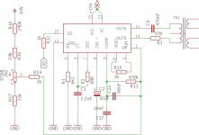
Can You check my SG3525 230V smps driver? It's stabilized +/-32V, but stabilization is connected between + and - output voltages (negative rail is connected to driver ground). The controller has a separated power supply 230V/15V. There's also a output couplet inductor, so output voltages would be equal.
I'm not sure if stabilization will work good. I meat the way of connection R13/R15 and C17/C22 and their values.
Circuit in attachment, sorry for my english")
Can You check my SG3525 230V smps driver? It's stabilized +/-32V, but stabilization is connected between + and - output voltages (negative rail is connected to driver ground). The controller has a separated power supply 230V/15V. There's also a output couplet inductor, so output voltages would be equal.
I'm not sure if stabilization will work good. I meat the way of connection R13/R15 and C17/C22 and their values.
Circuit in attachment, sorry for my english
Attachments
Hi... I guess, tell me if I am wrong, that this is going to be an offline converter and you will be using a half-bridge power stage driven by a pulse transformer, T1.
The following may or may not make sense but since you have mentioned the use or a Coupled Inductor I have faith.
In the first place it looks like you have connected the reference to the wrong input of the amplifier. It should go to the non-inverting input whilst the feedback goes to the inverting input.
Sometimes it can go the other way around but I think that is the right way in this case.
https://www.onsemi.com/pub/Collateral/SG3525A-D.PDF
The amplifier in the SG3525 is what is known as a transconductance amplifier.
A change in input voltage results in a change in output current. Look at Figure 8) and, in particular, Figure 5) which shows Cp and Rz converting that output current to a voltage for use with the PWM comparator.
In order to use it you do not implement local feedback 'around' the amplifier, your C22/R13, you just load the output with an appropriate network.
The starting point is to work out what the transconductance, gm, of the amplifier is. It does seem a bit silly that they do not give a figure for it but you can work it out from Figure 5).
Voltage Gain is 20dB, 10V/V, at 10KHz with Cp set to 1nF. The impedance of a 1nF capacitor at 10KHz is about 16K so to get 10V across it you need 10/16K or 625uA.
That makes the gm of the amplifier 625uA/V
There is a delightful 'trick' to compensating a system like this. I am not sure if it is widely publicised or known but it is derived from the concept of Slope Matching as used in Average Current Mode control.
https://e2echina.ti.com/cfs-file/__...-Mode-Control-of-Switching-Power-Supplies.pdf
This sets a maximum gain in the Error Amplifier at the switching frequency such that the slope of the output of the Error Amplifier does not exceed the Oscillator Ramp Slope at the inputs to the PWM comparator.
In Average Current Mode Control that slope arises from Output Filter Inductor current converted to a Voltage Ramp in the Current Sense Resistor.
By extension in Voltage Mode Control that slope arises from Output Filter Inductor current converted to a Voltage Ramp in the ESR of the Output Filter Capacitor{s}.
In this case you are looking at the period during the Switch Off Time when the output inductor is being Reset through VOUT and its current is ramping down. The Down Slope Current, converted to a voltage in the ESR and reduced by your feedback divider/resistors, gets converted to an Up Slope when passed through the Error Amplifier.
The last bit you need is the value of the PWM Ramp Upslope. Again the Data Sheet is rubbish here. It gives no values for Ramp Valley, Ramp Peak or Ramp Amplitude.
The closest you might get is... the current mirror matches 1:1 the current in the timing resistor, RT, and a guess that the current in RT is going to be (Vref - 0.6)/RT
Pulling that together... My Math may be broken but it should work. You or someone else should check.
Output Inductor Current Downslope
dIL/dT = VOUT/LOUT
Converted to a Voltage Downslope in the ESR
dVOUT/dT = ESR.dIL/dT
dVOUT/dT = ESR.VOUT/LOUT
Presented to the Input of the Error Amplifier {Trick}
dVINV/dT = VREF/VOUT x dVOUT/dT
dVINV/dT = VREF.ESR.VOUT/LOUT.VOUT
dVINV/dT = VREF.ESR/LOUT
Trick is your feedback divider is VREF/VOUT.
Converted to a Current at the Error Amplifier Output
dIERR/dT = gm.dVINV/dT
dIERR/dT = gm.VREF.ESR/LOUT
Converted to a Voltage across RZ, Figure 5)
dVERR/dT = RZ.dIERR/dT
dVERR/dT = RZ.gm.VREF.ESR/LOUT
This gets compared to the Ramp
dVRAMP/dT = IRt/Ct
and, for Slope Matching, the values should, almost but back off a bit, be the same.
dVERR/dT <= dVRAMP/dT
RZ.gm.VREF.ESR/LOUT <= IRt/Ct
RZ = LOUT.IRt/gm.VREF.ESR.Ct
The Application Note by Lloyd Dixon gives the Loop Crossover frequency, Fc, as being,
Fc = Fs/2πD
Equation 3) Page 4). If you follow that Application Note through and try the sums on a bit of paper you will see that that is the case.
Fs is the oscillator frequency.
Assume D is 100%/1 which is close for your half bridge, you get to, nominally, pick CP, Figure 5) of the Data Sheet, to give a corner frequency in conjunction with RZ at half that frequency.
CP = 1/2πFcRz
CP = 1/πFsRz
However you also have to take into account general tolerances and the biggest one in this case will be the ESR of the output Capacitor{s}.
As such you would design for Slope Matching with the maximum expected ESR, calculate CP to agree with the above and then increase CP by a factor of ESRmax/ESRmin.
Last edited:
Thank You for Your anaswer, Sir.
It's a lot of knowledge. Unfortunately, it's probably not my level
Yes, it's offilne half-bridge converter. I saw many SG3525 circuits and in the most cases, Vref is connected to non-inverting input (pin 2) and Vout to inverting input, but I dont know how it works in SG3525.
Should I connect comparator pin to ground with capacitor and resistor in series?
Oooops. My bad. When I looked at your circuit I got slightly confused with the label orientations on the error amplifier input terminals. You have got it the right way around.
Yes... the rest of my answer looks a bit complicated but, beyond the conceptual stuff, it is more or less just algebra if you can avoid getting too worried about the dT terms.
You may not think it is your level but if you know Ohms law and can do this sort of thing
V = IR
I = V/R
R = V/I
then it is really not very much above your level
Maybe things will make more sense if you play about with an example.
If you have not got a copy of LTSpice then...
LTspice | Design Center | Analog Devices
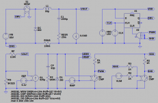
Your Half Bridge is a member of the family of Buck Converters. It is isolated but it works or behaves in the same way that a non-isolated Buck Converter does.
I have attached an 'ideal' model of one. Download the .asc file and open it in LTSpice.
Picture 1) is the circuit.
G1 represents your error amplifier with a forward transconductance, gm, of 625uA. CP and RZ are as shown in the 3825 data sheet. S2 is the PWM comparator with RMP being the Ramp.
There are some other things that you might ignore. S3 is a current limit comparator. Kind of like the Shut Down pin. SHD and PWM drive the latch, D-Type. In your half bridge things will be slightly different. I've used them here to stop the model losing the plot.
Otherwise the other component values plug into the equations given in my previous post apart from the IRt/C. That is the Ramp Slope. In the model this rises 3V in 9.5uS which is or would be the same as 100uA in Rt with Ct set to 317pF.
RZ = LOUT.IRt/gm.VREF.ESR.Ct
RZ = 64u.100u/625u.5V1.25m.317pF
RZ = 253K
With VIN 80V and VOUT 64V the duty cycle will be 0.8
Crossover Frequency.
Fc = Fs/2πD
Fc = 100E3/2π0.8
Fc = 19.89KHz
CP = 1/2πFcRz
CP = 1/πFsRz
I might have got that part wrong. Should have been...
CP = 2/2πFcRz
CP = 1/πFcRz
CP = 63pF
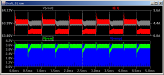
Picture 2) is the circuit in regulation with a 1A-5A load.
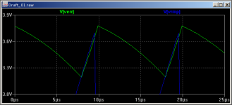
Picture 3) is the output of the error amplifier compared to the Ramp.
As suggested the goal is to achieve Slope Matching and then the rest falls into place. Again you have to worry about how things may be non-ideal or otherwise vary, in particular the ESR of the output capacitor.
Otherwise, as described, the method gives you the 'right' answer and the highest possible bandwidth for this type of converter.
Yes... the rest of my answer looks a bit complicated but, beyond the conceptual stuff, it is more or less just algebra if you can avoid getting too worried about the dT terms.
You may not think it is your level but if you know Ohms law and can do this sort of thing
V = IR
I = V/R
R = V/I
then it is really not very much above your level
Maybe things will make more sense if you play about with an example.
If you have not got a copy of LTSpice then...
LTspice | Design Center | Analog Devices
Your Half Bridge is a member of the family of Buck Converters. It is isolated but it works or behaves in the same way that a non-isolated Buck Converter does.
I have attached an 'ideal' model of one. Download the .asc file and open it in LTSpice.
Picture 1) is the circuit.
G1 represents your error amplifier with a forward transconductance, gm, of 625uA. CP and RZ are as shown in the 3825 data sheet. S2 is the PWM comparator with RMP being the Ramp.
There are some other things that you might ignore. S3 is a current limit comparator. Kind of like the Shut Down pin. SHD and PWM drive the latch, D-Type. In your half bridge things will be slightly different. I've used them here to stop the model losing the plot.
Otherwise the other component values plug into the equations given in my previous post apart from the IRt/C. That is the Ramp Slope. In the model this rises 3V in 9.5uS which is or would be the same as 100uA in Rt with Ct set to 317pF.
RZ = LOUT.IRt/gm.VREF.ESR.Ct
RZ = 64u.100u/625u.5V1.25m.317pF
RZ = 253K
With VIN 80V and VOUT 64V the duty cycle will be 0.8
Crossover Frequency.
Fc = Fs/2πD
Fc = 100E3/2π0.8
Fc = 19.89KHz
CP = 1/2πFcRz
CP = 1/πFsRz
I might have got that part wrong. Should have been...
CP = 2/2πFcRz
CP = 1/πFcRz
CP = 63pF
Picture 2) is the circuit in regulation with a 1A-5A load.
Picture 3) is the output of the error amplifier compared to the Ramp.
As suggested the goal is to achieve Slope Matching and then the rest falls into place. Again you have to worry about how things may be non-ideal or otherwise vary, in particular the ESR of the output capacitor.
Otherwise, as described, the method gives you the 'right' answer and the highest possible bandwidth for this type of converter.
Attachments
Yes.. Thanks.
Unless R14 makes it easier to lay out the board then it is not strictly needed. However it in combination with your feedback resistors presents an impedance to one input of the error amplifier.
Ideally you should present the same impedance to the other input, in your case R15, to balance and remove the error from input bias currents. Do not make R14 and R15 the same value.
As an approximation R17, 22K, dominates so R15 would be 22K. Of course since you have an adjustment in place you might not care so much but it is always nice to minimise sources of error as and when you can.
You might wish to consider not using the pot at least not as shown. It may be a minor concern but if the wiper goes bad you lose feedback. Make R17 too big and include the option to add a higher value, Adjust on Test, resistor in parallel with it.
R13/C17 are in the right place but you will need to calculate the correct values. I think you may know that but it looks like you have not yet finalised the complete circuit. You might choose to lay out the board with spaces for them and select them later.
Basically pick a 'silly' value for C17... 220n and a low value for R17 then, assuming you have a scope, measure the ripple/slope at the output of the error amplifier and compare it to the Ramp. Increase R17 until they almost match and then recalculate C17 based on the previous sums.
...Yes I often mix up 3525 and 3825. The latter is a similar but better and more flexible high speed controller.
Elsewhere in your circuit:
The gate drive components on the secondary side of the pulse transformer seem to be slightly confused.
Your current limit/shutdown transformer is not connected correctly and you might wish to consider using an LM393 instead of the LM324.
Your main transformer and the output inductor appear to be 'off the shelf components' or you have not as yet finalised them.
The following might be immensely incorrect. I am, almost, just plucking numbers out of the air based on 'intuition'.
Thinking about it again I got it even more wrong. Whilst both of your output rails add up to 64 Volts each rail works out to be 32V. I'll have to check out/remind myself about coupled inductors again but...
From the start/mains input.
With a 230VAC input your primary DC bus, after rectification, will be 325V peak with ripple determined by the bulk capacitance and load. Your 230VAC will be subject to tolerances and then you might have to design for a single cycle mains drop out.
All of these things can be determined but let's just assume that your minimum primary DC bus will be 300V.
With a Half Bridge you will apply 150V to the transformer Primary converted to something at the Secondary according to the turns ratio. Now you get into engineering, design, performance choices.
Ignore those and guess that for Minimum VIN your converter will be operating at 80% duty cycle. With VOUT at 32V the secondary voltage from the transformer will be 40V.
This is hand waving stuff but the turns ratio, Np/Nsec, of your transformer becomes 3.75:1.
Let's say your desired output current is 5A. More hand waving says the ripple in your output inductor 'should' be about 20% of the average or, in this case, 1A... change in current, dI.
Your circuit suggests that your target transformer frequency is 50KHz so the switching frequency is 100KHz, period of 10uS. At 80% duty cycle the Off time, Toff, is 2uS. This is when your output inductor gets reset through VOUT.
That lets you calculate its value as...
L = VOUT.Toff/dI
L = 32V.2uS/1A
L = 64uH
You show T131 as being 11.4uH/16A which would give you a ripple current of about 5.6A Again it looks like you have not finalised the design and are otherwise looking at, the possibly wrong, off the shelf components.
Going back to your main transformer your circuit indicates that you will be using an ETD39. At this sort of operating frequency, ignoring/using the possibility of flux doubling, considering core losses and you will have to look at the appropriate data sheet, you might choose to operate at a peak flux of 200mT. Peak to peak that becomes 400mT.
With a 150V drive and primary switch on time of 4uS you can work out the minimum primary turns as being...
NPMin = VIN.Ton/Ae.dB
Ae is the effective core area,
http://www.farnell.com/datasheets/1481602.pdf
125E-6
NPMin = 150V.4uS/125E-6.400mT
NPMin = 12
Call that 15 and your secondary turns, 3.75:1, becomes 4.
Then you have to chase around the houses selecting wire sizes. It is not trivial but, using lots of iteration, you can arrive at an answer.
Unless R14 makes it easier to lay out the board then it is not strictly needed. However it in combination with your feedback resistors presents an impedance to one input of the error amplifier.
Ideally you should present the same impedance to the other input, in your case R15, to balance and remove the error from input bias currents. Do not make R14 and R15 the same value.
As an approximation R17, 22K, dominates so R15 would be 22K. Of course since you have an adjustment in place you might not care so much but it is always nice to minimise sources of error as and when you can.
You might wish to consider not using the pot at least not as shown. It may be a minor concern but if the wiper goes bad you lose feedback. Make R17 too big and include the option to add a higher value, Adjust on Test, resistor in parallel with it.
R13/C17 are in the right place but you will need to calculate the correct values. I think you may know that but it looks like you have not yet finalised the complete circuit. You might choose to lay out the board with spaces for them and select them later.
Basically pick a 'silly' value for C17... 220n and a low value for R17 then, assuming you have a scope, measure the ripple/slope at the output of the error amplifier and compare it to the Ramp. Increase R17 until they almost match and then recalculate C17 based on the previous sums.
...Yes I often mix up 3525 and 3825. The latter is a similar but better and more flexible high speed controller.
Elsewhere in your circuit:
The gate drive components on the secondary side of the pulse transformer seem to be slightly confused.
Your current limit/shutdown transformer is not connected correctly and you might wish to consider using an LM393 instead of the LM324.
Your main transformer and the output inductor appear to be 'off the shelf components' or you have not as yet finalised them.
I saw something. You got 80V as Vin, so I guess You took 120VAC as supply voltage, while I use 230VAC, so Vin should be about 160V.
The following might be immensely incorrect. I am, almost, just plucking numbers out of the air based on 'intuition'.
Thinking about it again I got it even more wrong. Whilst both of your output rails add up to 64 Volts each rail works out to be 32V. I'll have to check out/remind myself about coupled inductors again but...
From the start/mains input.
With a 230VAC input your primary DC bus, after rectification, will be 325V peak with ripple determined by the bulk capacitance and load. Your 230VAC will be subject to tolerances and then you might have to design for a single cycle mains drop out.
All of these things can be determined but let's just assume that your minimum primary DC bus will be 300V.
With a Half Bridge you will apply 150V to the transformer Primary converted to something at the Secondary according to the turns ratio. Now you get into engineering, design, performance choices.
Ignore those and guess that for Minimum VIN your converter will be operating at 80% duty cycle. With VOUT at 32V the secondary voltage from the transformer will be 40V.
This is hand waving stuff but the turns ratio, Np/Nsec, of your transformer becomes 3.75:1.
Let's say your desired output current is 5A. More hand waving says the ripple in your output inductor 'should' be about 20% of the average or, in this case, 1A... change in current, dI.
Your circuit suggests that your target transformer frequency is 50KHz so the switching frequency is 100KHz, period of 10uS. At 80% duty cycle the Off time, Toff, is 2uS. This is when your output inductor gets reset through VOUT.
That lets you calculate its value as...
L = VOUT.Toff/dI
L = 32V.2uS/1A
L = 64uH
You show T131 as being 11.4uH/16A which would give you a ripple current of about 5.6A Again it looks like you have not finalised the design and are otherwise looking at, the possibly wrong, off the shelf components.
Going back to your main transformer your circuit indicates that you will be using an ETD39. At this sort of operating frequency, ignoring/using the possibility of flux doubling, considering core losses and you will have to look at the appropriate data sheet, you might choose to operate at a peak flux of 200mT. Peak to peak that becomes 400mT.
With a 150V drive and primary switch on time of 4uS you can work out the minimum primary turns as being...
NPMin = VIN.Ton/Ae.dB
Ae is the effective core area,
http://www.farnell.com/datasheets/1481602.pdf
125E-6
NPMin = 150V.4uS/125E-6.400mT
NPMin = 12
Call that 15 and your secondary turns, 3.75:1, becomes 4.
Then you have to chase around the houses selecting wire sizes. It is not trivial but, using lots of iteration, you can arrive at an answer.
Basically pick a 'silly' value for C17... 220n and a low value for R17 then, assuming you have a scope, measure the ripple/slope at the output of the error amplifier and compare it to the Ramp. Increase R17 until they almost match and then recalculate C17 based on the previous sums.
Unfortunately, I do not have an oscilloscope. But I could choose these values "on the ear" until the transformer stops making sound.
Your current limit/shutdown transformer is not connected correctly and you might wish to consider using an LM393 instead of the LM324.
Yea, I know there is something wrong with connections. But I don't know if using LM393 is required? I mean, if LM324 is to slow to shut down SG3525 on time?
You show T131 as being 11.4uH/16A which would give you a ripple current of about 5.6A Again it looks like you have not finalised the design and are otherwise looking at, the possibly wrong, off the shelf components.
I calculated T131 with this page:
Half-Bridge Push-Pull Converter
Vin_min = 280V
Vin_max = 338V
Vout = 32V
Iout = 16A (peak current, it's stereo amplifier supply, so: (32V/4R)*2 channels)
f = 50kHz
It gives me 11.13uH inducator, thats equal 17 turns on T131-8/90.
Going back to your main transformer your circuit indicates that you will be using an ETD39. At this sort of operating frequency, ignoring/using the possibility of flux doubling, considering core losses and you will have to look at the appropriate data sheet, you might choose to operate at a peak flux of 200mT. Peak to peak that becomes 400mT.
I assumed B=180mT (360mT peak-to-peak) bacause there's stablilization. I used to use that formula for years:
(Umax*10^6)/(2*f*Ae*B)
In this case it would be:
(169*10^6)/(2*50*125*180) = 75 turns (I winded 80).
OK... Your design page uses the same kind of calculations I would expect but it seems to adopt slightly different design criteria. My effort was incomplete but I would be concerned about operating at 40% ripple current in the inductor. However if that works out in terms of overall power loss... why not?
(Umax*10^6)/(2*f*Ae*B)
(169*10^6)/(2*50*125*180)
169 is presumably half your maximum primary DC Bus. 10^6 is to take care of uS, mT and kHz in the denominator and the 2 in the denominator moves the Transformer frequency of 50KHz to the Switching Frequency of 100KHz.
Some things to bear in mind.
Single ended converters, Forward, Flyback, operate in the first quadrant of the BH plot. Double ended converters, Half Bridge, Full Bridge, Push Pull, operate in the first and third quadrants of the BH plot.
The absolute limit is the saturation flux density of your core material. Somewhere about 350mT. Double ended the possible excursion is twice this or 700mT but depending on the transformer frequency you are likely to be core loss limited.
N87 Page 83/84
Note that this is peak flux. You use Pv with the effective volume of your core, Ve, to work out the core losses. Ve will be given for a core half in mm^3 so you have to double it and multiply it by 1E-9 to change it to cubic meters.
Page 525/526
Gives you core parameters including Ve for as an example ETD 39.
Page 168/169
Gives you thermal resistances for a fully wound core with convection cooling.
For a given ambient temperature and allowable temperature rise work out what power loss will be and assign half to the windings and half to the core. Unfortunately you then get into iteration with wire sizes and fit.
However when using the power loss, Pv, curves whilst with double ended converters you calculate primary turns using the peak to peak flux, 360mT, you enter the graph with half that value, 180mT.
(Umax*10^6)/(2*f*Ae*B)
(169*10^6)/(2*50*125*360)
You also have to take into account a load of other stuff mainly in terms of operating duty cycle worst case and in normal regulation which may or may not work in your favour.
I am used to designing transformers for low noise and end up losing space to interwinding screens so I would not expect to put 500W through an ETD39 and would chose a larger output inductor.
End of day a working result is a working result.
Oh.... as you probably know the LM393 is a 'proper' comparator so not only will its response time be faster, 200nS with 100mV overdrive, it is also a specified/know figure. The LM324 may work and could be easier to interface but there will not be much difference in cost.
(Umax*10^6)/(2*f*Ae*B)
(169*10^6)/(2*50*125*180)
169 is presumably half your maximum primary DC Bus. 10^6 is to take care of uS, mT and kHz in the denominator and the 2 in the denominator moves the Transformer frequency of 50KHz to the Switching Frequency of 100KHz.
Some things to bear in mind.
Single ended converters, Forward, Flyback, operate in the first quadrant of the BH plot. Double ended converters, Half Bridge, Full Bridge, Push Pull, operate in the first and third quadrants of the BH plot.
The absolute limit is the saturation flux density of your core material. Somewhere about 350mT. Double ended the possible excursion is twice this or 700mT but depending on the transformer frequency you are likely to be core loss limited.
N87 Page 83/84
Note that this is peak flux. You use Pv with the effective volume of your core, Ve, to work out the core losses. Ve will be given for a core half in mm^3 so you have to double it and multiply it by 1E-9 to change it to cubic meters.
Page 525/526
Gives you core parameters including Ve for as an example ETD 39.
Page 168/169
Gives you thermal resistances for a fully wound core with convection cooling.
For a given ambient temperature and allowable temperature rise work out what power loss will be and assign half to the windings and half to the core. Unfortunately you then get into iteration with wire sizes and fit.
However when using the power loss, Pv, curves whilst with double ended converters you calculate primary turns using the peak to peak flux, 360mT, you enter the graph with half that value, 180mT.
(Umax*10^6)/(2*f*Ae*B)
(169*10^6)/(2*50*125*360)
You also have to take into account a load of other stuff mainly in terms of operating duty cycle worst case and in normal regulation which may or may not work in your favour.
I am used to designing transformers for low noise and end up losing space to interwinding screens so I would not expect to put 500W through an ETD39 and would chose a larger output inductor.
End of day a working result is a working result.
Oh.... as you probably know the LM393 is a 'proper' comparator so not only will its response time be faster, 200nS with 100mV overdrive, it is also a specified/know figure. The LM324 may work and could be easier to interface but there will not be much difference in cost.
Last edited:
Oh.... as you probably know the LM393 is a 'proper' comparator so not only will its response time be faster, 200nS with 100mV overdrive, it is also a specified/know figure. The LM324 may work and could be easier to interface but there will not be much difference in cost.
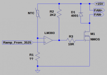
Problem is in the PCB layout. I don't have enought space to place two DIL8 chips. Btw, it's comparator with latch, so one pulse is enough to block SG3525.
I noticed the additional components around the LM324 to make it latch. LM358 is the dual LM324 but you can also get an LM392 which I believe is an LM358 type op-amp and LM393 type comparator in the same 8pin package.
http://www.ti.com/lit/ds/symlink/lm392-n.pdf
http://www.ti.com/lit/ds/symlink/lm392-n.pdf
Oh. Sorry... I missed the link to the data book on my previous post.
https://en.tdk.eu/download/519704/0...2ba503/ferrites-and-accessories-db-130501.pdf
https://en.tdk.eu/download/519704/0...2ba503/ferrites-and-accessories-db-130501.pdf
Excellent!
You would not normally try to use a comparator as a, linear, amplifier since they are designed to be inherently unstable. However it may be possible to implement some sort of self oscillating thing. Of course you might also consider using them as pulse width modulators given you already have a RAMP voltage available from the 3525.
You would not normally try to use a comparator as a, linear, amplifier since they are designed to be inherently unstable. However it may be possible to implement some sort of self oscillating thing. Of course you might also consider using them as pulse width modulators given you already have a RAMP voltage available from the 3525.
Of course you might also consider using them as pulse width modulators given you already have a RAMP voltage available from the 3525.
I don't have space, I used the rest of it for an additional chip. But since the SG3525 contains an amplifier in it, I would like to use it.
Tell me Sir, what do You finally think about the feedback circuit and output inducator? Can I leave it as it is or does it require any necessary modifications?
- Status
- This old topic is closed. If you want to reopen this topic, contact a moderator using the "Report Post" button.
- Home
- Amplifiers
- Power Supplies
- Please, check my SG3525 driver state