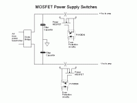
Your drawing shows depletion mosfets,the have to be turned off with sufficient negative gate voltage.The other (more common) type is normaly turned off and need a positive voltage on the gate to turn on.want to turn on and turn off the power supply using mosfets. I will be using a microcontroller to turn off the amp. Is there any way to do it?
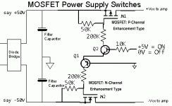
the following circuit doesnt work I have tried to simulate it.
Mona
It should work - I've rigged up a few and they do work. You need to pay attention to the polarity of the optocoupler output, and also make sure that the optocoupler can produce enough voltage to fully enhance the MOSFETs, and not provide too much to break down the gate relative to the source. Also make sure you're driving the LED properly - check the data sheet, but they generally want 10mA of drive, so get the resistor value right re. the LED's on voltage and your driving voltage. For example: (Vdrive - Vled)/0.01A = series resistor in ohms.
im using almost 0.1F per rail so there will be considerable charge left to which leads into the load and hence damages more.Why not use a couple of mosfets before the rectifier? If one power rail is disconnected it could damage the amplifier and/or speaker
I believe the second type is better to use as there wont be micro controller noise entering into it. Do you have any schematic which worked for you?Your drawing shows depletion mosfets,the have to be turned off with sufficient negative gate voltage.The other (more common) type is normaly turned off and need a positive voltage on the gate to turn on.
Mona
The photocouplers prevent microcontroller noise from having anything to do with anything - you get several thousand volts of galvanic isolation and only a tiny bit of capacitive coupling. Plus, if you get the right MOSFETs so that they are deeply enhanced when the photocoupler is on, any fluctuations in the LED current will not affect the conductivity of the MOSFET channel - t's already so enhanced that it can't be any further enhanced. The 0.1F of rail capacitance should also prevent problems.
Just get the basics of the circuit right and you'll be fine. The drawing you posted shows no series resistor into the photocoupler. You need one - see my first post on what value to make it.
Just get the basics of the circuit right and you'll be fine. The drawing you posted shows no series resistor into the photocoupler. You need one - see my first post on what value to make it.
Yes, equal to the product of the current through it and its "on resistance". You can get MOSFETs with very low on resistances now, 30mΩ for pretty small units and well under 1mΩ for larger ones. A typical 2A rated MOSFET (a tiny one) will probably have an on resistance of around 50mΩ. So, that'll be 50mW at 1A on current.
Look at the graph of Rds vs. Vgs in the datasheet and see how it varies with increasing Vgs. At a certain point, additional Vgs will decrease Rds very little, since the channel is almost completely enhanced. This is the region you want to drive a MOSFET to, since it will be maximally efficient.
The photocoupler will generate a voltage, usually around 7-8V, and initially, most of the charge generated is spent on charging the gate capacitance. After that's done, the voltage rises further, and gets to its ultimate value. So, look at the Rds versus Vgs graph and see what the value is at the open circuit output voltage rating of the photocoupler, and you can estimate these losses pretty accurately.
BTW, that photocoupler mentioned in the schematic you posted, the PV1050N, is long obsolete. Vishay and Toshiba make modern ones that you can actually buy. Digikey stocks them. I'd post a list, but my list is only of ultra-thin packaged versions for SMT that are truly annoying to use outside of a custom designed PCB. I dug around and here's a product selector from Toshiba: Photovoltaic-Output Photocouplers | TOSHIBA Semiconductor & Storage Products | Europe(EMEA) Cross reference that to Digikey's stock and you can find something that can actually be ordered.
Last edited:
but depletion mosfets which are available have little current ratings can be ok for 1 pair of output transistors rather than 6 or 7 pairs of output transistors.
I have checked the following case: Can anyone answer the following fault condition scenario.
1. One of the Positive and negative transistor is blow up and there is DC going into the load. Consider in that case using a Microcontroller we can cutoff the speaker load but we see the positive voltage is applied to the emitter of the bottom transistor (PNP). So my question is will it destroy the bottom transistor also? I am worried about the latched state of the mechanical relay which is used for the power supply cuttoff for both positive and negative.
2. I can use two relays one for positive voltage rail after the PSU caps and one mech relay for the negative. Mosfet based protection for the speaker. Now if one of the transistor blows off then the mosfet at the speaker will trigger off and the speaker is saved. Now when the positive transistor is blownup then the current will flow heavily into the negative side about all the current gets to the negative transistor also and hence I believe that will also burn out. So Im worried about the relay latch I will be using a 20Amp rated relay but will the relay latches up and burnup the whole amp PCB?
")
Don't use relays. MOSFETs are far more reliable. You can use two N channel enhancement mode MOSFET load switches for the power supply rails and they will both turn on and off at the same time. You want to turn both power supply rails, positive and negative, on or off, at the same time, regardless of the fault. With a relay, they will not switch at the same time, and that itself can cause problems, even if the amp circuitry is working properly.
To make a speaker load switch, you need to put two N channel enhancement MOSFETs connected back to back, with their sources connected together, one drain connected to the amp output, the other drain connected to the speaker load, and both gates connected in parallel, with the optocoupler driving the gate and source as normal, except that it's driving two MOSFETs instead of one.
Relays are tricky since the contacts can weld shut, preventing them from turning off. Every time they're used to switch current, you might burn a little spot away from the contact area, slowly increasing their on resistance. At the very least, unless you get really hard contacts, they deform every time you close the contacts, again degrading their on resistance. Finally, the time it takes to close or open the contacts is unknown and variable, depending upon a lot of silly factors. A MOSFET will simply switch the same now and 5 years from now, unless you blow it up. The on resistance can also be far far lower than a relay, often 10-100x lower resistance than most sensibly sized relays.
...using a microcontroller to turn off the amp. ... doesnt work....
"Doesn't work" is not clear. What does it do? What does it not do that you would like it to do? What is the difference?
I don't like fancy parts like those opto-couplers. It can be done with simple bipolar transistors and a few resistors, if you can afford P-type and N-type Enhancement MOSFETs. (Using only N-type gets messier.)
Attachments
Last edited:
I guess it's a matter of taste. An "odd" optocoupler makes a high side switch very predictable, using only N channel MOSFETs, whereas using a circuit like you posted requires P and N channel MOSFETs to behave the same, something that will never happen with silicon: electron and hole mobilities in P+ and N+ diffusions are not symmetric. I will say that your circuit is nicely simple, but it requires a quality P channel MOSFET, of similar characteristics to an N channel device, which I will contend is just as "hen's teeth" as an optocoupler. To each his own, but thanks for posting a relatively sane and compact driving circuit for the non optocoupler version. I'll certainly consider it!
Edit: at last glance, the "war on bipolar power supplies" has forced most work on P channel enhancement MOSFETs to lag behind modern N channel trench FETs, so that's why I feel that a goofy optocoupler makes things nicer overall. But, thanks again for posting a sane, simple circuit for using N and P MOSFET load switches. I need to dig into the modern offerings and see if there are any modern P channel devices that'll work well here.
Edit: at last glance, the "war on bipolar power supplies" has forced most work on P channel enhancement MOSFETs to lag behind modern N channel trench FETs, so that's why I feel that a goofy optocoupler makes things nicer overall. But, thanks again for posting a sane, simple circuit for using N and P MOSFET load switches. I need to dig into the modern offerings and see if there are any modern P channel devices that'll work well here.
Last edited:
I guess it's a matter of taste.
...requires a quality P channel MOSFET, of similar characteristics to an N channel device, which I will contend is just as "hen's teeth"...
If we all had the same taste, we'd all buy Sanyo boom-boxes.
DigiKey (therefore any large distributor) has a selection of hen-teeth. Yes, P-type choice is pathetic next to the N-mob, and P-type is fundamentally less-good than N-type. But it is only a switch. Super-size the jaws and contacts (or die), both sides will be "perfect enough". Can we afford "super-size"?
rhythmsandy has not said how big this trolly-motor is. I picked "100+W", so dual 50V supplies, <2A average 6Apk on 8r and <4A average 12Apk on 4r, actually doing speech/music so not really working hard most of the time. So I went to DigiKey for P-type >100V >8A thru-hole and sorted on price.
The $1.06 part has a package I have not used. Taking a +3dB price range, #1 seems to meet the dartboard specs for $1.34. #2 would serve a hi-Volt amp that never saw lo-Z, $1.55.
0.2 Ohms Rds On should be ample for a 8r-4r amplifier. If not, there's another page of choices up to $12, and some may be spiffier.
An equally beefy N-type should be trivial.
Switching times will not be equal for P and N, as you say. This might favor the opto-N-plan. However the MOSFET speed is probably not the limit; with my values, the resistive gate drive against gate C will dominate. Miller Effect will be large. The P-type will tend to have more C; you can over-buy an N-type to get near-similar gate Cs. I get very-roughly 1 milliSeconds response time.
Long ago I looked at that type opto and noted 'slow' response into big C. I don't have the specs here and they may have got better.
The logic interface is, obviously, about 1.2V threshold, "TTL" (if you remember). Maybe 1.1V to 1.4V over any likely parts and temps. While I show 5V drive, actually any CMOS micro-CPU on 3.3V will swing with ample margin. There's no Schmitt so be sure the swing is quick/clean; CPU fine but a raw thermistor isn't enough. The transistor specs are mostly "any", except they must stand-off the raw supply so the 10/$1 30V parts won't do for larger power amps; 100V parts are not expensive today.
Attachments
Last edited:
0.2ms turn on and 0.3ms turn off into 1000pF for the tlp3906.Long ago I looked at that type opto and noted 'slow' response into big C. I don't have the specs here and they may have got better.
Look at this one it seems working with very less dissipation with low Rds on mosfets with 7mohm Rdson.
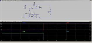
It feels right to me but when placed in the amplifier simulation the raise time is not sharp and it takes long time to raise. Just let me know if anything can be done to this circuit.
It feels right to me but when placed in the amplifier simulation the raise time is not sharp and it takes long time to raise. Just let me know if anything can be done to this circuit.
Attachments
- Status
- This old topic is closed. If you want to reopen this topic, contact a moderator using the "Report Post" button.
- Home
- Amplifiers
- Power Supplies
- Power supply +VCC -VEE turnoff using n ch mosfets?