You can use TL071's on a single supply. In fact any op-amp that has only two supply pins (like almost all of them) can run on a single supply, because the op-amp doesn't know what your ground reference is anyway.
You just have to check if the inputs and outputs can go close enough to the most negative supply voltage for your application. For example, when an op-amp's input common mode range is specified to be -11 V to +11 V at +/- 15 V supplies, that is exactly the same as stating that the inputs can handle +4 V to +26 V on a single-rail +30 V supply (from 4 V above the most negative to 4 V below the most positive supply).
Op-amps that are specifically designed to work on a single supply typically have in- and output stages that keep working at voltages quite close to ground, but as long as you don't need that, you can basically use any op-amp.
By the way, 90 megavolts is quite a change...
I had a little play at running the simulation as an 'AC' sim to show in real time the improvement the zener arrangement can bring but ran into unexpected stability issues.
I say unexpected... what seems to be happening is that I am asking to much of the opamp to drive a single transistor when the load current is high. So that needs looking at. A darlington (or FET) could be an ideal solution.
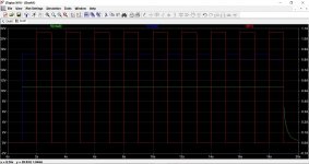
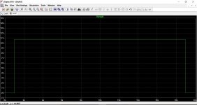
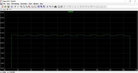
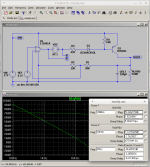
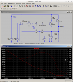
OK, so here is the simulation along with a switched load that is active and drawing current. The load is switched at 1Hz.
I also added series resistance to the supply to simulate the effect of the load current pulling the unregulated voltage down.
The first graph shows the raw supply in blue, the output voltage in green and the load current in red. Notice how the raw supply is now modulated by the load current.
The second graph is just the output voltage. Notice how steady it is as the load changes every second.
The third graph is with the zener fed off the raw supply (as you had it initially). The changes in raw supply now reflect into the zener current altering its absolute voltage level. This varying reference voltage is passed to the output as can be seen.
I say unexpected... what seems to be happening is that I am asking to much of the opamp to drive a single transistor when the load current is high. So that needs looking at. A darlington (or FET) could be an ideal solution.
OK, so here is the simulation along with a switched load that is active and drawing current. The load is switched at 1Hz.
I also added series resistance to the supply to simulate the effect of the load current pulling the unregulated voltage down.
The first graph shows the raw supply in blue, the output voltage in green and the load current in red. Notice how the raw supply is now modulated by the load current.
The second graph is just the output voltage. Notice how steady it is as the load changes every second.
The third graph is with the zener fed off the raw supply (as you had it initially). The changes in raw supply now reflect into the zener current altering its absolute voltage level. This varying reference voltage is passed to the output as can be seen.
Attachments
Mooly, I ran the set up with the zener, to the load and 10K resistor only with the LM741 and i got 66.5 millivolts it did not auto start. I tried the TL061 op amp and it also did not auto start. Next I added the resistor and diode with the 741 with the zener fed from the load as shown by marcelvdg and everything is very stable. I get the same 90 millivolt control as if the zener were being fed from the positive rail. I then tried the TL061 in the same set up and it would not auto start. Funny thing, I bumped wire from the collector to the emitter and the circuit began regulating with the TL061. I thought for sure I shorted out something and had one of my many "occurrences" but the circuit began conducting. When I turned off the power supply and tried to restart TL061 circuit it was a no go. Lastly, I can see how my original circuit input voltage variation can cause an output fluctuation.(graph 3) The Op amp must have been working like crazy to maintain a constant output voltage.
Maybe it's the common-mode input voltage range of the TL061. According to the datasheet, it is guaranteed to work from 4 V above the negative supply to 4 V below the positive supply, typically it's supposed to work from 3 V above the negative supply to the positive supply.
Because of the low start-up current, the voltage across your Zener might be less than 4 V or even less than 3 V at start-up. In that case a TL061 won't do anything.
Because of the low start-up current, the voltage across your Zener might be less than 4 V or even less than 3 V at start-up. In that case a TL061 won't do anything.
I've given it some thought... so much so I lashed the circuit up using a 741 and a TL082 and it is flaky in real life. With no load the circuit starts for me. With a 36 ohm load it does not. It also is unstable as anything and oscillates like crazy. A 47uF or higher cap on the output tames that but why so big ? Even more odd (to me) is that no amount of slapping caps around the opamp or feedback loop goes any way to stop this.
An old LM301 opamp with 100pF compensation cap seemed to work well however.
Very odd. I'm pleased though that the simulation also reveals the instability.
More thought required")
An old LM301 opamp with 100pF compensation cap seemed to work well however.
Very odd. I'm pleased though that the simulation also reveals the instability.
More thought required
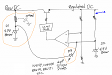
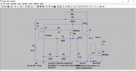
Mooly, you may want to investigate the startup circuit that Samuel Groner uses in his voltage regulator. I've shown the basic idea below, the startup items are circled in orange.
At the far right, Zener diode D2 supplies the reference voltage (4.7V) for the voltage regulator. The "purpose" of the startup components is to drag the noninverting input terminal of the opamp above ground, and nearly all the way to 4.7V, so that the opamp wakes up. Then the regulator regulates.
Zener diode D1 creates a second 4.7V reference voltage, using the RawDC supply instead of the RegulatedDC. Then D3 applies (4.7V minus DiodeDrop) to the opamp's noninverting input terminal, waking it up. When the regulator is regulating, D3 has 4.7V on both anode and cathode, and it does not conduct. D3 is off.
If you worry that D3 might fight against the enormous load connected to Regulated DC, you can prevent this fight by installing another PN diode (or a Schottky diode) at position "A". Now D3 cannot source current into the RegulatedDC line.
I suggest a low capacitance diode for D3, just so that any undesired "ick waveforms" (a/k/a "noise"), originating from RawDC and/or from D1, are not injected onto D2's cathode. A cheap 1N4148 diode has 4pF of capacitance; when you use a 2pF diode you get another factor of two reduction in "ick," with no increase in parts count.
_
Attachments
All, I never knew all these things could happen. Mark Johnson which way does the cathode go to prevent D3 cannot source current. Moody, I think maybe this design has too much instability and oscillation for use as a simple regulated filament heater circuit. Again, I keep learning from every comment here and I keep testing also. Thanks.
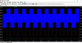
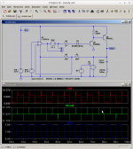
Thanks Mark. That's a novel start up method for sure The oscillation is more of a concern at the moment as can be seen here. The real build also behaves pretty much like this. A 100uF on the output tames it but that's about all that does.
I have an idea though.
The oscillation is more of a concern at the moment as can be seen here. The real build also behaves pretty much like this. A 100uF on the output tames it but that's about all that does.I have an idea though.
Attachments
All, I never knew all these things could happen. Mark Johnson which way does the cathode go to prevent D3 cannot source current. Moody, I think maybe this design has too much instability and oscillation for use as a simple regulated filament heater circuit. Again, I keep learning from every comment here and I keep testing also. Thanks.
It is to unstable, more so than I would have believed possible tbh.
Back to first principles me-thinks. Let me see what I can come up with.
Sigh Part 1)
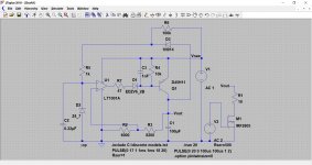
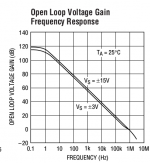
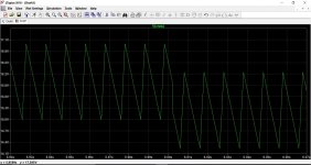
Latest circuit with spurious parts stripped out. The plot is of the loop gain.... Insert a 1V AC source in order to break the loop and plot V(a)/V(b).
It crosses 0dB at about 17KHz. The slope is 40dB/Decade which is second order. Phase is 0 Degrees.
You are operating the LT1001 without any local feedback. It introduces a DC pole and rolls off first order with a 90 degree lag. The D45H11 behaves as a current source driving the filter capacitance. Another DC pole with a 90 degree phase lag.
-180 degrees lag + -180 degrees feedback gives you 0 degrees phase margin and your circuit is unstable. If it were not for 'other things' it is likely that it would oscillate at about 17KHz.
Otherwise it turns itself into a sawtooth oscillator.
Attachments
I think most linear regulators are inherently unstable, its the nature of the beast, but what surprised me here was just how 'resistant' this one was to various measures thrown at it. That's why it needed a re-think.
So...
In post #1 mention was made of having a P channel power FET available. So lets use it. This allows two advantage to my way of thinking. The 'level shifting' zener can be dropped thanks to the higher Vgs needed to get the device to conduct (compared to traditional Vbe for the transistor) and most importantly, it relaxes the current demands on the opamp output which would be unable to support more than around 15ma. That's important for high load currents if we used a single series pass transistor.
To tame the stability we now have a small electrolytic on the regulator output. The feedback network also has a small cap added that seems to help under certain conditions.
This shows the output voltage (set to 12.6 volts) and a new 'noisy' raw supply which has both significant impedance and also simulated ripple superimposed on it.
The second graph shows the ripple at a transition where the load current is abrubtly applied.
Attachments
I think most linear regulators are inherently unstable, its the nature of the beast, but what surprised me here was just how 'resistant' this one was to various measures thrown at it. That's why it needed a re-think.
They are not though... as long as you, try to, compensate them.
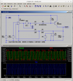
Here you go, someone can jump up and down on my head because I have no local feedback around the op-amp.
2 poles at 'DC'. One due to the op-amp one due to the D45H11 driving the output capacitor. ESR zero just above 10KHz. Crossover at about 50KHz with 60 degrees phase margin.
Attachments
2 poles at 'DC'
Would you explain, what is a pole at 'DC' ?
Does it mean that the open loop transfer function, expressed in the Laplace domain, includes a factor (s + 0) in the denominator?
Does it mean that the Bode plot slopes downward at -20dB/decade (-40dB if there are two such poles), at extremely low frequencies, frequencies so low that they are practically DC (say, below 1E-5 Hz)?
I have a feeling that I don't understand your meaning. Thanks!
If you wish to be pedantic then obviously below 1E-5Hz is not DC unless it is 0Hz. If you could care less then 0Hz is DC but if you did care less then I guess you would be talking about AC again.
Picture 1) A DC Pole.
Picture 2) Also a DC Pole.
I fail to understand why you wish to differentiate between Laplace and Bode or indeed any other representation or interpretation of 'things'. Ideally they are, or should be, equivalent.
Depending on how you feel or where you are one or the other, or indeed others, might give you more insight.
Let's stick with Bode Plots.
For others...
XC = 1/2πFC
but that does not take the associated phase shift into account..
XC = 1/j2πFC
Where j is the Square Root of -1 which does not exist so it is imaginary. Then you turn 2πF into ω to get
XC = 1/jωC
and substitute s for j because we are being Laplace dudes to get
XC = 1/sωC
Spot the difference? Me neither.
Avoiding the other stuff. j, or s, is a 90° phase lead. 1/j, or 1/s, is a 90° phase lag... -90°
Multiply top and bottom by Square Root of -1. Square Root of -1 X Square Root of -1 is -1.
XC = -s/ωC
s is a 90° phase lead. -s is a 90° phase lag, -90°
So Mark. How do you wish to proceed?
Attachments
Last edited:
Would you explain, what is a pole at 'DC' ?
Does it mean that the open loop transfer function, expressed in the Laplace domain, includes a factor (s + 0) in the denominator?
Does it mean that the Bode plot slopes downward at -20dB/decade (-40dB if there are two such poles), at extremely low frequencies, frequencies so low that they are practically DC (say, below 1E-5 Hz)?
I have a feeling that I don't understand your meaning. Thanks!
From the context I guess it must be a factor s + alpha, with the modulus of alpha so small you might as well neglect it. That is, modulus of alpha much smaller than the natural frequency omega_n of the loop.
XC = 1/jωC
and substitute s for j because we are being Laplace dudes to get
XC = 1/sωC
Spot the difference? Me neither.
Avoiding the other stuff. j, or s, is a 90° phase lead. 1/j, or 1/s, is a 90° phase lag... -90°
Under stationary sine wave excitation you can substitute jω for s, but you don't substitute j for s. That is, XC = 1/sC, not XC = 1/sωC.
- Status
- This old topic is closed. If you want to reopen this topic, contact a moderator using the "Report Post" button.
- Home
- Amplifiers
- Power Supplies
- Op amp Linear power supply