I have a question concerning the following. I am only a small time self taught hobbiest. I have a 741 op amp driving a TIP 102 NPN Darlington current pass transistor. I have two loads attached. One load draws .240 amps. The second load draws 1.150 amps. I can set the voltage output for the first load at 11.8 volts. When i switch the to the 1.150 amp load the voltage drops by almost .3 to .5 volts. My supply is 15 VDC. I use a 50 ohm resistor for the .240 Amp load and a 10 ohm resistor of for the 1.150 amp load. The transistors are heatsink mounted when testing. The heatsink temperature rises from about 23C to 77C with the higher amperage load. I also tried a PNP TIP 147 darlington and while it functions better suffers from the same larger than expected voltage drop changing from one load to the another. I have 2.4 to 3.2 volts on each darlington from collector to emitter so i think these are in saturation. I used the darligntons due to the op amp output current. The spec sheet says i only need about 300 microamps to get then current output. So, I tested a IRF9540 P channel mosfet with the same two loads and it holds within .04 volts regardless of load. Regulation from cold to hot is almost 99% accurate. Same temperature rise on the heatsink with the mosfet. I think I am operating the mosfet in saturation, but just barely.
Please help with any explanation as to why the darlington are losing, (not regulating) the voltage between current loads and any improvements I can make to allow the use of the darligntons. Regulation changes with an increase in temperature. How can I fix this too. I don't care whether I use NPN or PNP because they are inexpensive. Thanks.
Please help with any explanation as to why the darlington are losing, (not regulating) the voltage between current loads and any improvements I can make to allow the use of the darligntons. Regulation changes with an increase in temperature. How can I fix this too. I don't care whether I use NPN or PNP because they are inexpensive. Thanks.
why the darlington are losing, (not regulating) the voltage between current loads
Can you post a schematic?
I still challenge anyone to beat this supply for $10!!
LM317 / LM337 +/-1.5V~37V Adjustable Dual Voltage Regulator Power Board | eBay
LM317 / LM337 +/-1.5V~37V Adjustable Dual Voltage Regulator Power Board | eBay
I still challenge anyone to beat this supply for $10!!
LM317 / LM337 +/-1.5V~37V Adjustable Dual Voltage Regulator Power Board | eBay
Do you have schematics of this power supply?
It is attractive for lower cost and good presentation, but what is the function of the DIP8 operational amplifier as it have 2 voltage adjusts for positive and negative rail voltage. (supposed some kind of noise filter)
One problem of this kind of symmetrical regulator is the lack of protection systems to turn off both regulators when one fails.
Regards
Ronaldo
Historically PNPs were double the cost at lesser specs than NPNs.Please help with any explanation as to why the darlington are losing, (not regulating) the voltage between current loads and any improvements I can make to allow the use of the darligntons. Regulation changes with an increase in temperature. How can I fix this too. I don't care whether I use NPN or PNP because they are inexpensive. Thanks.
You are probably running out of "headroom" E.g. the voltage difference required between regulators pass input and the output and still remain in "regulation" under all operating conditions.( low line voltage, etc )
1) The regulators Vinput drops under load.
Consider the raw DC voltage will drop under load and it has AC ripple on it/. you can measure or estimate both. You must subtract from the average DC the lowest ripple valley. E.g. negative peak AC ripple component under full load is technically the correct Vin. Its normal to have 1 Vrms ripple at full load which is about 2.8 V peak-peak, so it's very possible for this to be worse if the bulk filter caps are wimpy.
2) The regulator needs the V error op-amp's output level and current to support the transistors Vbe's and any beta droop.
Look at the devices data sheets to calculate the level drop starting at the Op-amps Vout thru two Vbe's of the darlington. Next look at the op-amp current needed to support the full load. One trick is to tie the op-amps supply a few volts higher than the raw DC. The op-amps output current could still be too weak. But it's better to test it and see what headroom you have 1st. I'd suggest drop the output voltage by 2 or 3 volts and recheck.
Things to consider , either all or in combination of.
a) Use a beefier' Xfmr and filter capacitor.
b) Use a better op-amp and /or run it from a higher voltage.
c) Check the pass and driver transistors betas. Change the whole topology for "low drop out" performance. one thing you said a MOSFET pass element works with your op-amp and reference, right?
d) Reduce your specs E.g Output current and voltage to account for poor headroom. (this is the easiest solution)
Last edited:
http://www.diyaudio.com/forums/power-supplies/313648-lm317-load-capacitance-34.html#post5263905
.
See those circuits. They specially disigned for low noise application. MIC preamp, RIAA, playback amp, DAC converters.
.
.
See those circuits. They specially disigned for low noise application. MIC preamp, RIAA, playback amp, DAC converters.
.
You make a reference to the spec sheet for the Darlingtons. Did you consider the spec sheet for the operational amplifier?
http://www.ti.com/lit/ds/symlink/lm741.pdf
Check the output voltage specifications. Page 5) 6.5] Minimum output swing is +/-12V.
As infinia mentions your NPN will drop an extra 1.2V so it will likely be slightly rubbish. Your PNP may be better because you gain an extra 1.2V, pull down to turn it on. The P-Channel mosfet will be happiest of the three because the gate will need to be about 3V/5V below source for it to start conducting. It will also need less drive.
You also need to check Fb/Ft for your chosen transistors.
Also the 741 only has a Gain Bandwidth Product of 1MHz
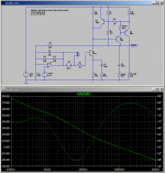
The following is an 'idealised' LTSpice model which may give you some ideas about how to do it. Also includes a 'concept' of foldback current limiting. It also lets you check the Loop Gain. Plot V(A)/V(B).
Loop stability is important.
http://www.ti.com/lit/ds/symlink/lm741.pdf
Check the output voltage specifications. Page 5) 6.5] Minimum output swing is +/-12V.
As infinia mentions your NPN will drop an extra 1.2V so it will likely be slightly rubbish. Your PNP may be better because you gain an extra 1.2V, pull down to turn it on. The P-Channel mosfet will be happiest of the three because the gate will need to be about 3V/5V below source for it to start conducting. It will also need less drive.
You also need to check Fb/Ft for your chosen transistors.
Also the 741 only has a Gain Bandwidth Product of 1MHz
The following is an 'idealised' LTSpice model which may give you some ideas about how to do it. Also includes a 'concept' of foldback current limiting. It also lets you check the Loop Gain. Plot V(A)/V(B).
Loop stability is important.
Code:
Version 4
SHEET 1 1224 832
WIRE 288 -240 -576 -240
WIRE 384 -240 288 -240
WIRE 480 -240 384 -240
WIRE 752 -240 480 -240
WIRE 288 -208 288 -240
WIRE 480 -208 480 -240
WIRE 752 -208 752 -240
WIRE 384 -96 384 -240
WIRE 480 -48 480 -128
WIRE 480 -48 448 -48
WIRE 528 -48 480 -48
WIRE 640 -48 608 -48
WIRE 752 -48 752 -128
WIRE 752 -48 640 -48
WIRE 640 -16 640 -48
WIRE 288 32 288 -128
WIRE 384 32 384 0
WIRE 384 32 288 32
WIRE 480 48 480 -48
WIRE 752 48 752 -48
WIRE 640 96 640 64
WIRE 688 96 640 96
WIRE 640 128 640 96
WIRE 288 176 288 32
WIRE 576 176 288 176
WIRE -304 256 -448 256
WIRE 480 256 480 128
WIRE 480 256 -224 256
WIRE 624 256 480 256
WIRE 640 256 640 224
WIRE 640 256 624 256
WIRE 752 256 752 144
WIRE 752 256 640 256
WIRE 784 256 752 256
WIRE 288 304 288 176
WIRE -448 352 -448 256
WIRE -304 352 -448 352
WIRE -96 352 -240 352
WIRE 80 352 -96 352
WIRE 224 352 192 352
WIRE 80 384 48 384
WIRE -448 432 -448 352
WIRE -368 432 -448 432
WIRE -240 432 -304 432
WIRE -96 432 -96 352
WIRE -96 432 -176 432
WIRE 288 448 288 400
WIRE 400 448 288 448
WIRE 400 480 400 448
WIRE 624 480 624 256
WIRE -448 496 -448 432
WIRE -304 496 -448 496
WIRE -96 512 -96 432
WIRE -96 512 -240 512
WIRE -64 512 -96 512
WIRE 48 512 48 384
WIRE 48 512 16 512
WIRE 80 512 48 512
WIRE 192 512 192 352
WIRE 192 512 160 512
WIRE -304 528 -336 528
WIRE -576 592 -576 -240
WIRE -448 592 -448 496
WIRE -336 592 -336 528
WIRE 288 592 288 448
WIRE 400 592 400 544
WIRE 624 592 624 544
WIRE 752 592 752 256
WIRE -576 704 -576 672
WIRE -448 704 -448 672
WIRE -448 704 -576 704
WIRE -336 704 -336 672
WIRE -336 704 -448 704
WIRE 288 704 288 672
WIRE 288 704 -336 704
WIRE 400 704 400 672
WIRE 400 704 288 704
WIRE 624 704 624 672
WIRE 624 704 400 704
WIRE 752 704 752 672
WIRE 752 704 624 704
WIRE -576 736 -576 704
FLAG -576 736 0
FLAG 784 256 VOUT
IOPIN 784 256 Out
FLAG 80 352 A
IOPIN 80 352 Out
FLAG 80 384 B
IOPIN 80 384 Out
SYMBOL pnp 688 144 M180
WINDOW 0 74 61 Left 2
WINDOW 3 75 37 Left 2
SYMATTR InstName Q1
SYMBOL pnp 576 224 M180
WINDOW 0 60 57 Left 2
WINDOW 3 62 32 Left 2
SYMATTR InstName Q2
SYMBOL res 624 -32 R0
WINDOW 0 39 43 Left 2
WINDOW 3 48 70 Left 2
SYMATTR InstName RDAR
SYMATTR Value 4K7
SYMBOL res 736 -224 R0
WINDOW 0 37 52 Left 2
SYMATTR InstName R10
SYMATTR Value 500m
SYMBOL res 272 -224 R0
WINDOW 0 39 55 Left 2
SYMATTR InstName R6
SYMATTR Value 10K
SYMBOL npn 224 304 R0
WINDOW 3 57 58 Left 2
SYMATTR InstName Q3
SYMBOL res 272 576 R0
WINDOW 0 38 55 Left 2
WINDOW 3 39 76 Left 2
SYMATTR InstName R4
SYMATTR Value 10K
SYMBOL res 176 496 R90
WINDOW 0 0 56 VBottom 2
WINDOW 3 32 56 VTop 2
SYMATTR InstName R3
SYMATTR Value 1K
SYMBOL cap 608 480 R0
WINDOW 0 44 19 Left 2
WINDOW 3 45 40 Left 2
SYMATTR InstName C3
SYMATTR Value 220µ
SYMBOL voltage -336 576 R0
WINDOW 0 41 44 Left 2
WINDOW 3 39 68 Left 2
WINDOW 123 0 0 Left 2
WINDOW 39 0 0 Left 2
SYMATTR InstName VREF
SYMATTR Value 2.5V
SYMBOL res -208 240 R90
WINDOW 0 0 56 VBottom 2
WINDOW 3 32 56 VTop 2
SYMATTR InstName R2
SYMATTR Value 8K2
SYMBOL cap -240 336 R90
WINDOW 0 0 32 VBottom 2
WINDOW 3 32 32 VTop 2
SYMATTR InstName C1
SYMATTR Value 39p
SYMBOL res -464 576 R0
WINDOW 0 36 47 Left 2
WINDOW 3 35 69 Left 2
SYMATTR InstName R1
SYMATTR Value 2K2
SYMBOL voltage -576 576 R0
WINDOW 0 44 48 Left 2
WINDOW 3 43 71 Left 2
SYMATTR InstName VCC
SYMATTR Value 15V
SYMBOL res 736 576 R0
WINDOW 0 34 49 Left 2
WINDOW 3 32 75 Left 2
SYMATTR InstName RLOAD
SYMATTR Value 10R
SYMBOL voltage 32 512 R90
WINDOW 0 -32 56 VBottom 2
WINDOW 3 32 56 VTop 2
WINDOW 123 60 59 VBottom 2
WINDOW 39 0 0 Left 2
SYMATTR InstName V1
SYMATTR Value ""
SYMATTR Value2 AC 1
SYMBOL res 608 576 R0
WINDOW 0 38 53 Left 2
WINDOW 3 42 76 Left 2
SYMATTR InstName RESR
SYMATTR Value 50m
SYMBOL res 624 -64 R90
WINDOW 0 0 56 VBottom 2
WINDOW 3 32 56 VTop 2
SYMATTR InstName R9
SYMATTR Value 1K
SYMBOL res 464 -224 R0
WINDOW 0 36 53 Left 2
SYMATTR InstName R7
SYMATTR Value 1K
SYMBOL pnp 448 0 R180
WINDOW 0 100 62 Left 2
WINDOW 3 76 33 Left 2
SYMATTR InstName Q4
SYMBOL Opamps\\opamp -272 448 R0
SYMATTR InstName U1
SYMATTR SpiceLine2 GBW=1Meg
SYMBOL diode -176 416 R90
WINDOW 0 0 32 VBottom 2
WINDOW 3 32 32 VTop 2
SYMATTR InstName D1
SYMATTR Value ZID
SYMBOL diode -368 416 M90
WINDOW 0 0 32 VBottom 2
WINDOW 3 32 32 VTop 2
SYMATTR InstName D2
SYMATTR Value ZID
SYMBOL cap 384 480 R0
WINDOW 0 43 23 Left 2
WINDOW 3 43 49 Left 2
SYMATTR InstName C2
SYMATTR Value 100n
SYMBOL res 384 576 R0
WINDOW 0 39 53 Left 2
SYMATTR InstName R5
SYMATTR Value 470R
SYMBOL res 464 32 R0
WINDOW 0 38 42 Left 2
WINDOW 3 40 66 Left 2
SYMATTR InstName R8
SYMATTR Value 10K
TEXT -536 792 Left 2 !.LIB OPAMP.SUB
TEXT -536 816 Left 2 !.ac dec 50 100 1E6
TEXT -536 768 Left 2 !.MODEL ZID D(Ron=10m Roff=1E9 Vrev=5V)
Attachments
LF353 provides feedback to lower noise.Do you have schematics of this power supply?
....... but what is the function of the DIP8 operational amplifier as it have 2 voltage adjusts for positive and negative rail voltage. (supposed some kind of noise filter)
Attachments
Can you post a schematic?
This is the most important point. We need to see the circuit to advise.
The most important points are that the output voltage itself is monitored and included within the feedback loop to the opamp. Secondly, if using an NPN pass transistor then you must ensure that there is sufficient headroom available for the opamp which simply means 'is the supply voltage high enough'.
If those points are covered then the circuit should show no appreciable change in output voltage with varying load.
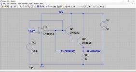
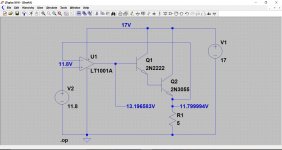
Here are the two scenarios. See how the opamp output voltage is quite high in the second example as it looks to drive the darlington pair.
Attachments
The most important thing is the measured voltages DC + AC under load.
The schematic alone wont tell us were the problem is. From the OP symptoms points to what the fundamental problem is, loses regulation under load. The best advise was to lower the output voltage until it regains regulation, If it doesn't happen then the circuit is broken. Infact he could use a potentiometer to determine the required headroom for any reasonable Vreg schematic. I agree schematics are helpful but necessarily mandatory given the OP's level and experience.
The schematic alone wont tell us were the problem is. From the OP symptoms points to what the fundamental problem is, loses regulation under load. The best advise was to lower the output voltage until it regains regulation, If it doesn't happen then the circuit is broken. Infact he could use a potentiometer to determine the required headroom for any reasonable Vreg schematic. I agree schematics are helpful but necessarily mandatory given the OP's level and experience.
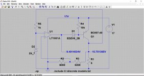
These are the schematics of what I am using fo
View attachment Voltage Regulator Circuits.pdf
r experimentation.
Infinia, I get perfect regulation regardless of load at about 9.8 Vout with the TIP147 or TIP 42C. I notice the Vce drops to about 2.3 to 3 volts. I read this as moving slightly out of satusartion and maybe this could be causing Vout to droop with the TIP 147 and TIP42C. There is zero affect using the IRF 9540 P channel mosfet. I mentioned I am just a hobbyist. I read something and then experiment on my breadboard to see if I can make it work. I struggle with the the why it works and why it does not work question. I do not have a dual rail supply only a fixed voltage 15 volt 2.5amp supply.
In the case of bipolar pass topology, note 741 error amp must rely on high state to drive the bipolar pass element, which looking at the data sheet Voh ~ 2 to 3V drop for a 10K/1mA load*. On top of that you must add both junction drops from the darlington to get the minimum headroom. This can be ~ 3.5V or more. Note the data sheet numbers are measured without fine grained linearity, E.g the error amp is resting at the stops. So call it ~4 volts of headroom. So the target regulator output voltage s/b less than or equal 11.0 Vdc Not counting any wiring drops or ripple, which can be significant when looking at millivolt changes at 1.3A. So youre reporting Vce ~ 2.3 -3 Volts which is much less than my rough estimate of 3.5-4.0 headroom, right? Consider to take more careful measurements. Are you sure there isn't AC ripple or wiring drops on your 15V source?
The MOSFET pass element works with less headroom because the 741 pulls the gate lower to drive the output harder. So 741 Voh/Vol is not at the end stops, it remains linear.
*worst case 741 load is Ib ~ Iout/Beta 1.3A /1000 or 1.3mA
The MOSFET pass element works with less headroom because the 741 pulls the gate lower to drive the output harder. So 741 Voh/Vol is not at the end stops, it remains linear.
*worst case 741 load is Ib ~ Iout/Beta 1.3A /1000 or 1.3mA
Last edited:
Infinia, I get perfect regulation regardless of load at about 9.8 Vout with the TIP147 or TIP 42C. I notice the Vce drops to about 2.3 to 3 volts.
Vout+Vce = Vin
9.8+3.0 =12.8 V so your Vin is not 15V anymore.
Last edited:
Try adding a zener (say 6.2v or thereabouts) in series with the base drive, and also add a B-E resistor of around 10k.
The PNP series pass transistor begins to turn on when the 741 output drops 600mv below the incoming supply... which is no good. The FET version overcomes that by reason of the FET having a high turn on voltage.
Also, the 3.9v zener is liable to fluctuation due to the incoming unregulated supply varying under load/ripple and should therefore be configured to be biased from the regulated output.
Attachments
Mooly, I tried the circuit you sent and it worked with one exception. I could not get the 3.9 volt zener to conduct/regulate from the regulated output so I connected it back to the V+ rail. Vout regulation is within .01 volt across the load conditions with a TIP 42c, and it did not matter if the circuit was cold or hot. Vout remains steady. I tried the TIP147 darlington and it could not manage the regulation across the load. Vout varied over 2 volts from the 50 ohm to 10 ohm load. I also changed out the 3.9 volt zener for a 4.7 Volt zener as I thought your circuit wanted me to do that. Here are more questions. What does the 6.2 volt zener do along with the 10K resistor? Why did the darlington not regulate as perfectly as the TIP 42C? Can this circuit work for NPN transistor use by moving the inverting and non inverting op amp connections and the V+ accordingly on the NPN?
Thanks again.
Thanks again.
Easy ones first...
I had not got a 3.9 volt model for the simulator so I used a 4.7 volt.
The 10k resistor guarantees the transistor base does not 'float' under any conditions. Its just good practice really. If the 6.2 volt zener was non conducting, and if the transistor was a high gain (or darlington) device then unexpected things might happen without the resistor.
The 6.2 volt zener is non critical, an LED or 8.2v or 2.7v zener should all work. All it does is force the opamp output to operate away from the positive rail.
For example, if the unregulated rail is 17 volts then the transistor will fully conduct when the base is pulled just 700mv or so below that value. That means the opamp output has to operate in the 17v to 16.3 volt region, something most opamps won't do. So we force it to work in the centre of its range by adding a 'volt drop' to the output. Now the opamp has to go below 6.2 +0.7 volts before the transistor conducts. So the opamp is happy and the opamp output is now at around 7 volts in normal operation.
The circuit should work feeding the zener from the output. Could the basic circuit be oscillating ? A scope check would show any problem there.
You could try adding a 10uF across the regulated output which would be good practice anyway. Also try a small cap (say 0.1uF) across the zener, again good practice.
If the circuit was oscillating then we cold look at a small cap across the feedback network.
Another odd problem that can occur in some circuits is 'failure to start'. If you had no output voltage when initially switched on then that could be a possibility... if you had voltage and it appeared just not to be regulating then oscillation is much more likely.
I would try the zener connected back to the output again and see if you can get it to work by adding the caps.
An NPN transistor can be used as long as there is enough 'headroom' or voltage differential between unregulated input and the regulated output voltage. 17 volts supply and 12 volts output leaves just 5 volts to play with. If you used a darlington NPN then you would need at least 13.4 or so drive voltage... and we are getting close to the supply. The PNP has no such restriction, we can pull the base as low as needed. PNP is the correct choice usually (for a positive regulator).
...I had not got a 3.9 volt model for the simulator so I used a 4.7 volt.....
You may already know this; or it may be difficult in your software....
Depending on your sim interface....
I use Edit, Model, Model text, and change the 4.7 to 13 or 3.9 as needed.
This will not be exact in all cases. The shape of the knee varies, especially from Zener to Avalanche zone. But to just set a voltage, or offset an opamp output, it works good enough for most cases.
Attachments

- Status
- This old topic is closed. If you want to reopen this topic, contact a moderator using the "Report Post" button.
- Home
- Amplifiers
- Power Supplies
- Op amp Linear power supply