The data sheet (MF linked in post №136) gives f(-3dB) values for high-speed mode (1.5MHz) and high-precision mode (10kHz).
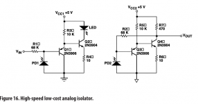
The specified circuit environments for the high-speed case is quite interesting, as the transmitter and receiver circuits are formed from a pair of 2N3904/3906 discrete transistors (data sheet figure 16) - which have good LTSPICE models.
Perhaps modelling this circuit and examining f(3) will offer a useful comparision with the data-sheet typical value of 1.5MHz. If it's much different, the coupler's model is suspect.
Last edited:
I did a comparison with MF's photovoltaic setup to my earlier photoconductive (biased diodes) and the difference is clearly that nasty bump with the fast phase rotation. So there is something in the model that does this.
I think I read that the input capacitance is 12pF but not sure if that was the LED or the diodes. Will see if I can find it.
Anyway, it seems that my complete circuit with the opto in photovoltaic mode is much more stable and might still have enough bandwidth for audio. Onward!
I am grateful for the education and ideas from MF, RC and MvdG!
Jan
Thanks. I had noticed those. There is also...
https://www.edn.com/Pdf/ViewPdf?contentItemId=4431092
SPICE Circuit Simulations for HCNR200 Analog Optocoupler (1476 KB)
The low speed circuits use the LM158/LM358 and as you say the high speed circuits are discrete. You would not expect much from an LM158.
Broadcom seems happy with the accuracy of the results but it would appear the limitations lie in what is used to drive the device/model rather than the device/model itself.
I guess the LT1028 is managing to push the limits of the device/model in about the same way the discrete solutions do... or perhaps that should be the other way around.
I suppose the jury might still be out.
In wet finger waving territory the nasty bump, input to output, is possibly an accumulation of poles due to diode capacitances and there might not be much that can be done about it...
I guess I have to explain why I make a fuss about the bump.
A bump in the magnitude of the transfer with a relatively fast -180 degrees jump in the phase indicates a complex pole pair in the left half plane with Q >> 1/2 sqrt(2). A quite complex left-half-plane pole pair far above the desired signal bandwidth is no problem if and only if you are sure the poles always remain in the left half plane.
Two things that can cause complex left-half-plane pole pairs are simple passive resonators, like an LC tank, and feedback loops with only little phase margin. The poles of an LC tank remain in the left half plane as long as the damping resistance stays positive. However, I don't see any inductors in MorbidFractal's variant of Jan's schematic (nor in the original), so it is more likely to be a feedback loop with only little phase margin.
There are two feedback loops. MorbidFractal's simulations show quite clearly that the first feedback loop, the LED driver, has plenty of phase margin after the modifications, so it must be the second feedback loop. If one can somehow establish that the phase margin of this loop remains positive under all circumstances, then the poles remain in the left half plane and there is again no problem, but establishing that is difficult without corner models. Hence, I feel uncomfortable about such a bump.
On top of that, as MorbidFractal already mentioned in post 136, there is the behaviour of an overall loop over the whole thing, if indeed Jan wants to enclose the whole circuit in such a loop. Unless there are lots of strategically placed compensation zeros available, such a loop will tend to push the poles further towards the right half plane (no matter where they originate from).
Last edited:
FWIIW...
My most recent test suggested I might be able to do this so I did and it does raise further questions as to the accuracy of the model. It is 'idealised' but all I have done is cancelled what might be the LED capacitance. It makes no difference what mode the photodiodes are operated in.
My most recent test suggested I might be able to do this so I did and it does raise further questions as to the accuracy of the model. It is 'idealised' but all I have done is cancelled what might be the LED capacitance. It makes no difference what mode the photodiodes are operated in.
Attachments
Only me again...
I checked the reverse bias capacitance on the diodes. Zero bias 8pF, agrees with model internals. -15V about 16pF. It is almost as if it is not worth having.
Looking back at some of the circuit responses I have developed a concern about what might be happening with device capacitances messing about with opamp nodes.
In particular the diodes should ideally be terminated into short circuits which is something the opamp current to voltage converter is meant to achieve. Then there is drive of the LED itself.
What about current mode feedback amplifiers? I have looked at them in the past but cannot claim any in depth knowledge other than they are possibly used in diode stuff and they are meant to be fast...
The inverting input is purportedly low impedance and other stuff. So I come up with...
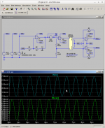
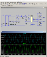
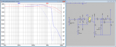
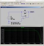
Picture 1) U1, CFB, implement a classic voltage to current converter to drive the LED. As is the case in Spice I have fiddled about with things and it turns out that R3 is needed to stop it banging off at 100MHz.
Not sure why but the inverting input is the low impedance node and R3 might be isolating the LED capacitance. This is making things up mode.
U2 and U3, CFB, are the photodiode current to voltage converters. Again the inverting terminal is the low impedance node. Again I've messed about with R5/R6 to get something that works. It might be worth reading about how feedback works in these things but it is slightly beyond me.
U4, VFB, is the linearising amplifier comparing output of the primary photodiode to the demand signal, VIN. You really need to break the circuit down and play about yourself to get some idea as to what might be going on.
I have just intuitively made 'best effort'.
The plot is supposedly loop gain of the primary side linearising loop, U4 and U1, V(a)/V(b). It is much prettier than the previous efforts. I guess U4 is allowed to do its proposed job better whilst U1 handles the grunt work.
Picture 2) This is the input to output response. -3dB at about 3.5MHz. There is some slight gain peaking that is tweakable via R2 and C1.
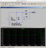
Picture 3) 1KHz transient.
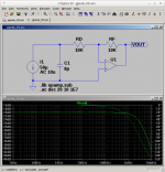
Picture 4) 1MHz transient.
In the case of 4) you can see the gain peaking.
I have sort of forgotten but U1 appeared to be functional up to about 10MHz so, if you wish to be mad and have more, things still seem to be limited by the LT1028. I am sure that will still be pushing things.
Overall in terms of responses things look cleaner. Still silly bandwidths though.
Other files attached if you want to play. I have 'cheated' on the .lib and .asy so you will have to rename them as required and place them in the right directories for LTSpice to find and use them.
I checked the reverse bias capacitance on the diodes. Zero bias 8pF, agrees with model internals. -15V about 16pF. It is almost as if it is not worth having.
Looking back at some of the circuit responses I have developed a concern about what might be happening with device capacitances messing about with opamp nodes.
In particular the diodes should ideally be terminated into short circuits which is something the opamp current to voltage converter is meant to achieve. Then there is drive of the LED itself.
What about current mode feedback amplifiers? I have looked at them in the past but cannot claim any in depth knowledge other than they are possibly used in diode stuff and they are meant to be fast...
The inverting input is purportedly low impedance and other stuff. So I come up with...
Picture 1) U1, CFB, implement a classic voltage to current converter to drive the LED. As is the case in Spice I have fiddled about with things and it turns out that R3 is needed to stop it banging off at 100MHz.
Not sure why but the inverting input is the low impedance node and R3 might be isolating the LED capacitance. This is making things up mode.
U2 and U3, CFB, are the photodiode current to voltage converters. Again the inverting terminal is the low impedance node. Again I've messed about with R5/R6 to get something that works. It might be worth reading about how feedback works in these things but it is slightly beyond me.
U4, VFB, is the linearising amplifier comparing output of the primary photodiode to the demand signal, VIN. You really need to break the circuit down and play about yourself to get some idea as to what might be going on.
I have just intuitively made 'best effort'.
The plot is supposedly loop gain of the primary side linearising loop, U4 and U1, V(a)/V(b). It is much prettier than the previous efforts. I guess U4 is allowed to do its proposed job better whilst U1 handles the grunt work.
Picture 2) This is the input to output response. -3dB at about 3.5MHz. There is some slight gain peaking that is tweakable via R2 and C1.
Picture 3) 1KHz transient.
Picture 4) 1MHz transient.
In the case of 4) you can see the gain peaking.
I have sort of forgotten but U1 appeared to be functional up to about 10MHz so, if you wish to be mad and have more, things still seem to be limited by the LT1028. I am sure that will still be pushing things.
Overall in terms of responses things look cleaner. Still silly bandwidths though.
Other files attached if you want to play. I have 'cheated' on the .lib and .asy so you will have to rename them as required and place them in the right directories for LTSpice to find and use them.
Attachments
-
cnr200.asc4.1 KB · Views: 28
-
 Screenshot at 2018-01-21 13:06:30.png51.7 KB · Views: 55
 -
 Screenshot at 2018-01-21 13:00:06.png52.1 KB · Views: 125
 -
 Screenshot at 2018-01-21 12:55:49.png52.1 KB · Views: 129
 -
 Screenshot at 2018-01-21 12:54:41.png51.6 KB · Views: 137
 -
cnr200lib.txt1.1 KB · Views: 31
-
cnr200asy.txt473 bytes · Views: 33
Last edited:
Whoah! Where do you guys get the time to do all this??
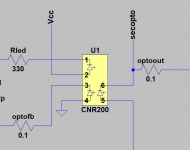
I worked on it some today. Got sick of wondering whether I got the right connections on the CNR200 so made a more expressive symbol, attached. You may need to edit the file path property to point it to where your model is at. Rename to CNR200.asy of course.
I also played with the opamp type. On the secondary side I see a lot of impact on the response connecting the opto-output to the non-inv. input. All of a sudden there is that kink at about 2MHz. This is open loop. I'll see if I can attach some plots.
Jan
Attachments
Last edited:
FWIIW...
My most recent test suggested I might be able to do this so I did and it does raise further questions as to the accuracy of the model. It is 'idealised' but all I have done is cancelled what might be the LED capacitance. It makes no difference what mode the photodiodes are operated in.
MF, the I(B1) graph rises at frequency, is that not the LED input cap at work?
Jan
Gain Peaking in an I to V converter.
Some words to the thoughts.
I had mentioned the possibility and that was based on something in the back of my head mentioned somewhere else.
Picture 1) Classic I to V converter circuit.
The input current source represents the photo-diode.
Picture 2) Classic I to V converter with diode capacitance.
Voltage gain is RF/RIN.... Guess What?
Picture 3) Adding input resistance to tame things.
Without thinking harder, flying in the fog, I have no idea what the trade offs might be.
Oh.. your new .asy looks like the old .asy but you might see from my circuits that I have being messing about with the .asy to get pretty circuits. Right click, open symbol, mess about and save.
Attachments
MF, the I(B1) graph rises at frequency, is that not the LED input cap at work?
Jan
B1 is a behavioural current source whose output current is set to follow the current in V1. The load on V1 is set to increase current drawn and cancel the effects of diode, LED/Photo, capacitance.
")
Oh.. your new .asy looks like the old .asy but you might see from my circuits that I have being messing about with the .asy to get pretty circuits. Right click, open symbol, mess about and save.
Hmmm. How about this?
Attachments
B1 is a behavioural current source whose output current is set to follow the current in V1. The load on V1 is set to increase current drawn and cancel the effects of diode, LED/Photo, capacitance.
Right. Got it.
Jan
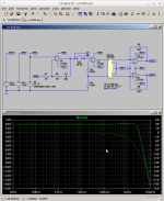
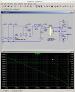
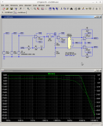
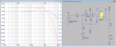
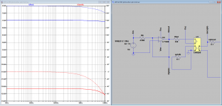
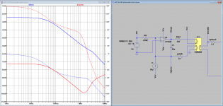
That '1MHz bump' originates (of course) in the input circuit, because that is the only place with feedback.
If you look at the open loop response between the input LED and the input photodiode, they show nice 1st order behaviour (fig 1). Yet if you connect them up in a loop it gets funny (fig 2).
I am seeing MvdG this weekend, see if he can make chocolate from it (which I am sure he can!).
Jan
If you look at the open loop response between the input LED and the input photodiode, they show nice 1st order behaviour (fig 1). Yet if you connect them up in a loop it gets funny (fig 2).
I am seeing MvdG this weekend, see if he can make chocolate from it (which I am sure he can!).
Jan
Attachments
All, I just added a new bench power supply today. I will experiment more, but have to stay to the basics. I find all of this interesting and could have never guessed in 63 years that power supplies are so complicated. The original circuit I started with was posted not he internet and thus started my path of experimentation and trying to understand the "why" it either worked or did not work. Thanks again.
I still challenge anyone to beat this supply for $10!!
LM317 / LM337 +/-1.5V~37V Adjustable Dual Voltage Regulator Power Board | eBay
This might for USD 6.53 - EA - Low Noise Dual Variable DC Regulated +/- 2.5V To +/-30V PSU EADPS02 – Eight Audio(R)
- Status
- This old topic is closed. If you want to reopen this topic, contact a moderator using the "Report Post" button.
- Home
- Amplifiers
- Power Supplies
- Op amp Linear power supply