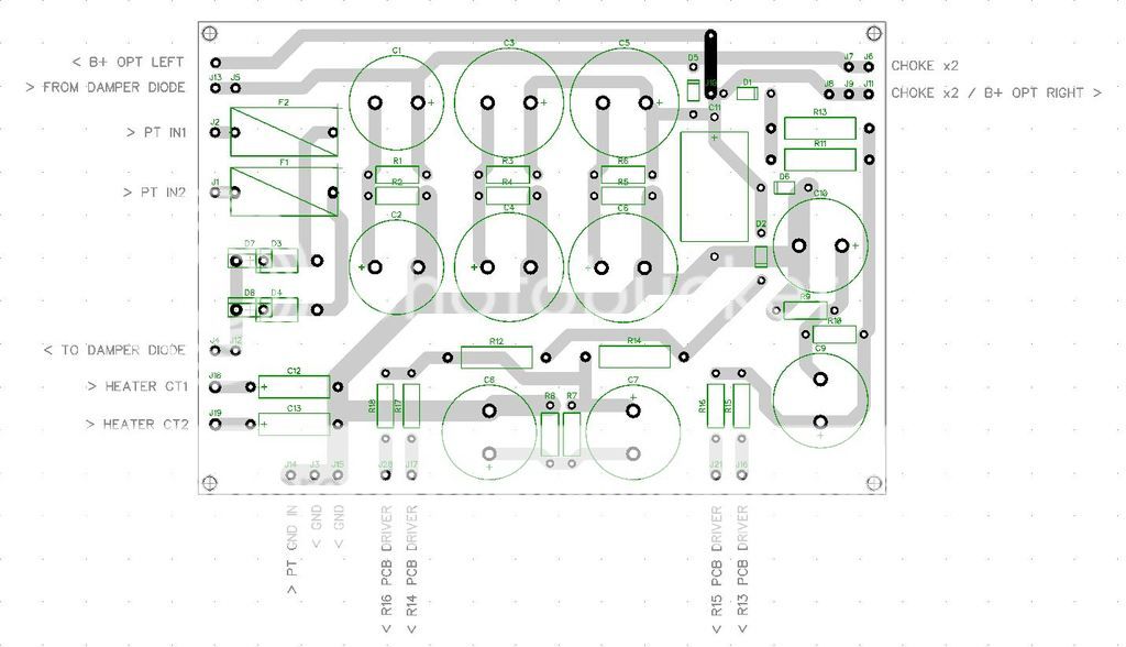
Hello all,
Did i overdoit with the thickness of the traces ?
I'm building a power supply for a tube amp, and i don't know what thickness should be. In the picture bellow i used a 5mm for GND and 3mm for the rest. A few info about the amp, it will have 4 kt88 tubes and 3 12au7 tubes, B+ will be ~500v, 240 ma + driver board 30ma.
A definite no I would say. I would also look to making pads larger, much much larger. Think how big a fuseholder pins are for instance. Connections to the outside world need to be big and robust.
Have a look at post #22 and 23 here. Big big big and with plenty of copper.
GERMANIUM Single ended Class A Headphone Amp.
Have a look at post #22 and 23 here. Big big big and with plenty of copper.
GERMANIUM Single ended Class A Headphone Amp.
Hello all,
Did i overdoit with the thickness of the traces ?
I'm building a power supply for a tube amp, and i don't know what thickness should be.
No, you didn't over-do-it. Thicker (actually, wider. Trace thickness is in a different dimension) traces exhibit lower resistance. Think about the vast majority of PCBs featuring a ground plane, which is simply an widest possible trace giving the lowest resistance.
Last edited:
Definitely not, make them as big as you can (it's free after all) while maintaining the minimum clearance for safety based on the voltage you are operating at.
Pads (for wiring) should have plenty of copper, 4 - 5mm dia is not unreasonable if you have the space..
The power transformer CT should be connected right to the ground end of the very first cap string in the filter if you want to minimize charging current modulation of the trace resistances. As designed not good.
Did i overdoit with the thickness of the traces ?
Thin traces are ok for the DC balancing resistors.
In general, make each pad's diameter three times its hole diameter,
if possible.
Last edited:
Personally, I think the traces are wide enough.
I would make the *pads* a LOT bigger. As big as will fit. Then when you get actual parts (or have to replace them in 2027) and the lead-spacing is different than you figured, you can re-drill and it will fit.
Also those minimal size pads are not very robust. Maybe you plan to treat your stuff nice. But DIY debugging is often a lot of yanking to get boards in and out for testing.
You don't pay for the copper you use. You pay for the whole board of copper! Use it!
Attachments
Last edited:
It uses more ferric chloride to remove the copper so leave as much on as possible.
Thicker copper means lower impedance tracks.
Fill copper out as much as possible but keep clearances enough for what ever voltage the track has on it.
If you don't want to increase pad sizes just fill in around pads with tracks.
Thicker copper means lower impedance tracks.
Fill copper out as much as possible but keep clearances enough for what ever voltage the track has on it.
If you don't want to increase pad sizes just fill in around pads with tracks.
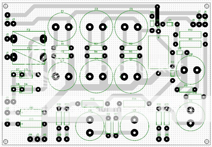
Thank you all for answering. I was living with the impression that wider traces introduce higher resistance...
I have enough space so I've made the pads 3 times the hole diameter.
I would like to play with copper pour option for GND. What would be a minimum clearance between traces? taking into account that i will have between 380-500v on the board.
Thanks.
I have enough space so I've made the pads 3 times the hole diameter.
I would like to play with copper pour option for GND. What would be a minimum clearance between traces? taking into account that i will have between 380-500v on the board.
Thanks.
Whoa! Go back to school man!Thank you all for answering. I was living with the impression that wider traces introduce higher resistance...
")
Some info on spacing here:
IPC-2221B PCB Trace Spacing / Clearance by Voltage
Its often not as much as you think although in practice I think you need to consider humidity, altitude and whether the board is coated in a conformal coating.
I believe uncoated glass fibre PCB would come in at around 2.5mm spacing for up to 500 volts and below 10,000ft
I was living with the impression that wider traces introduce higher resistance.
Think of a wide trace as a number of thin traces in parallel. The multiple paths mean
less total resistance to current flow. Mathematically, the resistance of a trace is
proportional to the length, and also is inversely proportional to the width.
Thank you all for answering. I was living with the impression that wider traces introduce higher resistance...
Resistance is based on ohms per square of a copper sheet of a certain weight. Wider traces have lower number of squares for a fixed distance, so resistance is lowered.
https://www.edn.com/electronics-blo...sistance-of-a-copper-trace--Rule-of-Thumb--14
Since you have higher voltages, current is small, so resistance can be very much not a factor here.
PCB re workability is important. also Consider parts to trace spacing's in 3 dimensions. Re Top side traces pads going under snap-in caps etc, large caps have metal cans covered in plastic with unknown or non guaranteed dielectric properties.I have enough space so I've made the pads 3 times the hole diameter.
No not necessary. Can actually cause many more problems than any gains, esp. on power supplies and tube gear. Advise , a strong Nope.I would like to play with copper pour option for GND. What would be a minimum clearance between traces? taking into account that i will have between 380-500v on the board.
Last edited:
Hi franciscano,
I would make the holes in the donuts smaller than they are. Otherwise you may end up in the unhappy situation where you have no copper to solder to, kind of like a moat around the component lead. What you need is a way to accurately place the hole, it is more than okay to drill into copper.
-Chris
I would make the holes in the donuts smaller than they are. Otherwise you may end up in the unhappy situation where you have no copper to solder to, kind of like a moat around the component lead. What you need is a way to accurately place the hole, it is more than okay to drill into copper.
-Chris
You can deliberately move the pad from the centre of the hole.
A wider pad on one side makes for easier solder tip placement to start heating the pad before you roll the tip across the heat the component lead.
To make use of this asymmetrical pad/hole arrangement, you need to visualise the space the soldering iron needs to get in and provide the elongated pad on the side for soldering after some components are placed.
- Status
- This old topic is closed. If you want to reopen this topic, contact a moderator using the "Report Post" button.
- Home
- Amplifiers
- Power Supplies
- Did i over do it with the thickness of the traces ?