Hi.
I'm a newbie at SMPS and LLC in particular, but with the aid of the app-note An1160 I have managed to get a simple LLC prototype running. I don´t claim to understand every calculation in the PDF, but I put it all into a spreadsheet and it puts out values that are similar to the values calculated in the example.
https://www.infineon.com/dgdl/an-1160.pdf?fileId=5546d462533600a40153559a85df1115
The target is to power a bridged amp with +/-30V driving a single 8Ohm speaker to around 150W (100Vpp).
So peak-current is around 7A, and average is like 1A for music
I'm using a L6599 controller in a standard setup, IRFP450 (overkill, but I had them), and a ATX-transformer-core with a airgap in the center-leg.
Transformer x-section is around 1cm2 and prim-sec windings are side-by-side to integrate all magnetics into one. I have tried dual, triple and littze-wire for primary and although it changed the internal heating a little it does not affect the output power
The LLC works great up until approx 60V into a 22Ohm dummy-load (60^2/22 = 160W).
But when its loaded with 12Ohm (60V/12Ohm = 5A) for just 10mS the voltage drops to around 40-45V and it struggles to maintain soft switching.
Now the ATX-core and the windings will probably never supply 60V@7A for more than short pulses before the heat rises, but it needs to supply the peaks in the sine.
I have tried different resonant-caps and different airgaps. This result in different minimum switch-freq to maintain soft-switching, but it dos not affect maximum output current by much. Also tried to add more sc-windings with little luck.
Depending on the airgap the prim inductance is around 500uH (250uH with shorted sec). Prim-inductance can go from 1500uH to 250uH with airgaps from 0.1 to 1mm with around 50 prim turns.
So, any ideas?
Kind regards TroelsM
small update.
Maybe part of the problem was that I had placed the AUX-winding (psu for the L6599) over the primary winding. The AUX-voltage rose way too high during high loads on the sec.
With the AUX winding over the sec winding the voltage on the AUX should be semi-regulated as well.
Problem is that the isolation-distances are much better when AUX is placed over prim.
Whats the normal here?
Kind regards TroelsM
well I found a app-note that deals a little more with the actual construction of the LLC transformer:
https://www.onsemi.com/pub/Collateral/AND8460-D.PDF
See page 17 to 21.
PLacing the gap under the primary makes construction a little harder as one have to cut and glue the ATX-psu transformer-core, but I think it can be done.
I have had some luck with cutting ferrite with a small ebay diamond-disc in a dremmel.
Kind regards TroelsM
Magnetics design is hard. LLC magnetics design is evil. LLC operation and feedback compensation is critical in respect of the magnetics design.
If your transformer parameters do not match your design parameters then things will fall over and it is very hard to get the transformer to match. You might notice mention is often made of 'cut and try'...
You might want to try using an external inductor with a tightly coupled 'transformer' rather than integrating it into the transformer itself. The method is suggested in many application notes but people wish to play hardball and save money...
Otherwise you might care to look at,
http://www.ti.com/lit/ml/slup105/slup105.pdf
http://www.ti.com/lit/ml/slup103/slup103.pdf
Just in case I am not allowed to post links yet search Google for "sepic Lloyd Dixon" and "coupled inductor Lloyd Dixon".
to get some idea as to what is going on. I really know nothing myself but basically leakage inductance is uncoupled energy between windings. With the caveat that I know nothing then I would be slightly dubious about location of the gap.
I do not doubt that it will have an effect but as to how it might be quantified is another issue... 'cut and try'. Stray flux can be dealt with by the use of an external shield foil. However rather than trying to chop things to move the gap it would be easier to make the primary winding longer than the secondary so the primary overlaps the gap and the secondary misses it.
In respect of isolation of your primary auxiliary whilst maintaining some concept of regulation you might consider triple insulated wire. Otherwise given the primary auxiliary is likely to be low power waste the overvoltage in a resistor and zener diode regulator.
You mention that you are using an ATX transformer core which suggests that you have taken something from a junked computer power supply. That could/will be a source of grief because you do not know what the core parameters really are.
This might actually work in your favour assuming it is already an LLC transformer. Someone has already designed the transformer with 12V windings. Take it to bits, identify the 12V windings and put them back in place with three times as many turns.
Unfortunately now you have to match your proposed control circuitry to that used by the supply.
Looking back at the Lloyd Dixon application note he suggests a target of 2mH/200uH or 10% leakage inductance. Your On Semi application note suggests 750uH/130uH or about 17%.
If you read about LLC and try to get your head about things the the ratios determine the range of regulation and peak currents along with other things. Again I am no expert but going for a wide range results in greater circulating currents and higher losses.
However the difference between what Dixon achieves and what On Semi imply to be a suitable solution is not excessive. Basically, assuming 'like for like', you can just double the space between the windings and you should/might be close.
One thing that has always bothered me is that in the description of coupled inductors it is apparent that positioning of the leakage inductance is important in order to achieve the required ripple current steering.
I am not sure how that might apply to a transformer but would guess that either you assume that in that case it is symmetrical
or, just to be safe, place it in series with the primary. That seems to go against what On Semi suggests in respect of location of the gap... Whatever.
You are still going to get problems if you are using 'any old core'. It, it's gap and the windings have to be designed to hit your specification. That may or may not work with 'any old core' but, for the moment, that's another story.
Hi. Thank you for the long answer. I really appreciate it.
My findings so far: With the ATX-core, a 3mm seperator in the middle of the bobbin and a 1-2mm gap in the center-leg the inductance-ratio between becomes approx 1:2.
The app-notes and design-calculators I looked at suggest that the primary-inductance shall be lower for higher output. This puzzled me in the beginning, but now I'm thinking that the inductance needs to be low in order for the primary-current to rise enough?
The calculators suggest that the primary-windings shall be calculated like for an un-gapped Xformer based on the voltage the windings will see. This gives approx 50-60 windings for a core with 1cm2 cross-section. But that drives the inductance way up.
So I tried with fewer windings and a gap of 1,5mm. 30 windings appears to e good compromise. -iddle heat is low. Heat at 60W output is luke-warm and it will do peaks of 500W without sagging in output voltage.
Inductance is approx:
I have not calculated or simulated the entire feedback-loop. From what I have seen it looks very complicated, so I just copied the feedback-loop from a similar design.
So far it handles all, load-changes I tested with.
Kind regards TroelsM
My findings so far: With the ATX-core, a 3mm seperator in the middle of the bobbin and a 1-2mm gap in the center-leg the inductance-ratio between becomes approx 1:2.
The app-notes and design-calculators I looked at suggest that the primary-inductance shall be lower for higher output. This puzzled me in the beginning, but now I'm thinking that the inductance needs to be low in order for the primary-current to rise enough?
The calculators suggest that the primary-windings shall be calculated like for an un-gapped Xformer based on the voltage the windings will see. This gives approx 50-60 windings for a core with 1cm2 cross-section. But that drives the inductance way up.
So I tried with fewer windings and a gap of 1,5mm. 30 windings appears to e good compromise. -iddle heat is low. Heat at 60W output is luke-warm and it will do peaks of 500W without sagging in output voltage.
Inductance is approx:
An externally hosted image should be here but it was not working when we last tested it.
I have not calculated or simulated the entire feedback-loop. From what I have seen it looks very complicated, so I just copied the feedback-loop from a similar design.
So far it handles all, load-changes I tested with.
Kind regards TroelsM
Data is a good thing to have. One of the best in respect of ferrites would be,
https://en.tdk.eu/download/519704/0...2ba503/ferrites-and-accessories-db-130501.pdf
Siemens -> Epcos -> TDK
Rather than using a Junk core think about buying one that fits your requirements.
I have already mentioned I do not know enough but I have looked at LLC converters in the past using LTSpice. If I try to recreate it, this for the moment is incomplete...
Copy the text and save it as an .asc file. LTSpice should open it.
Might look like the attached picture and I think you will be able to guess as to what is going on.
https://en.tdk.eu/download/519704/0...2ba503/ferrites-and-accessories-db-130501.pdf
Siemens -> Epcos -> TDK
Rather than using a Junk core think about buying one that fits your requirements.
I have already mentioned I do not know enough but I have looked at LLC converters in the past using LTSpice. If I try to recreate it, this for the moment is incomplete...
Code:
Version 4
SHEET 1 1128 932
WIRE -64 32 -416 32
WIRE 16 32 -64 32
WIRE 112 32 16 32
WIRE 240 32 208 32
WIRE 352 32 320 32
WIRE 544 32 432 32
WIRE 672 32 608 32
WIRE 736 32 672 32
WIRE 848 32 736 32
WIRE 880 32 848 32
WIRE -64 96 -64 32
WIRE 16 96 16 32
WIRE 112 96 112 32
WIRE -112 112 -192 112
WIRE 432 112 432 32
WIRE 544 112 432 112
WIRE 640 112 608 112
WIRE 352 144 352 32
WIRE 432 144 432 112
WIRE -112 160 -160 160
WIRE -416 192 -416 32
WIRE -64 224 -64 176
WIRE 16 224 16 160
WIRE 16 224 -64 224
WIRE 112 224 112 160
WIRE 112 224 16 224
WIRE 208 224 208 32
WIRE 208 224 112 224
WIRE 352 256 352 224
WIRE 432 256 432 224
WIRE 544 256 432 256
WIRE 640 256 640 112
WIRE 640 256 608 256
WIRE 736 256 736 32
WIRE 848 256 848 32
WIRE -64 272 -64 224
WIRE 16 272 16 224
WIRE 112 272 112 224
WIRE -112 288 -192 288
WIRE -160 336 -160 160
WIRE -112 336 -160 336
WIRE 432 336 432 256
WIRE 544 336 432 336
WIRE 672 336 672 32
WIRE 672 336 608 336
WIRE -416 400 -416 272
WIRE -160 400 -160 336
WIRE -160 400 -416 400
WIRE -64 400 -64 352
WIRE -64 400 -160 400
WIRE 16 400 16 336
WIRE 16 400 -64 400
WIRE 112 400 112 336
WIRE 112 400 16 400
WIRE 352 400 352 320
WIRE 352 400 112 400
WIRE 640 400 640 256
WIRE 640 400 352 400
WIRE 736 400 736 320
WIRE 736 400 640 400
WIRE 848 400 848 336
WIRE 848 400 736 400
WIRE -416 432 -416 400
WIRE 160 432 -80 432
WIRE -208 464 -240 464
WIRE -304 480 -336 480
WIRE -208 480 -208 464
WIRE -208 480 -240 480
WIRE -208 496 -208 480
WIRE -208 496 -240 496
WIRE -208 512 -208 496
WIRE -208 512 -240 512
WIRE -32 528 -240 528
WIRE 160 528 160 432
WIRE 160 528 128 528
WIRE 368 544 336 544
WIRE 400 544 368 544
WIRE 496 544 464 544
WIRE 608 544 576 544
WIRE 640 544 608 544
WIRE 736 544 704 544
WIRE 848 544 816 544
WIRE 880 544 848 544
WIRE -80 576 -80 432
WIRE -80 576 -240 576
WIRE -48 576 -80 576
WIRE 160 576 128 576
WIRE 192 576 160 576
WIRE -304 592 -336 592
WIRE -208 592 -208 512
WIRE -208 592 -240 592
WIRE -208 608 -208 592
WIRE -208 608 -240 608
WIRE -208 624 -208 608
WIRE -208 624 -240 624
WIRE 368 624 368 544
WIRE 400 624 368 624
WIRE 608 624 608 544
WIRE 608 624 464 624
WIRE -208 640 -208 624
WIRE -208 640 -240 640
WIRE 32 672 0 672
WIRE 160 672 160 576
WIRE 160 672 32 672
WIRE 608 672 608 624
WIRE 608 672 576 672
WIRE 672 672 608 672
WIRE 736 672 672 672
WIRE 848 672 848 544
WIRE 848 672 816 672
WIRE -208 688 -208 640
WIRE -64 688 -208 688
WIRE 32 688 32 672
WIRE 32 688 0 688
WIRE 368 688 368 624
WIRE 512 688 368 688
WIRE 32 704 32 688
WIRE 32 704 0 704
WIRE 608 704 576 704
WIRE 32 720 32 704
WIRE 32 720 0 720
WIRE 32 736 0 736
WIRE 160 736 160 672
WIRE 160 736 96 736
WIRE 368 736 368 688
WIRE 400 736 368 736
WIRE 608 736 608 704
WIRE 672 736 672 672
WIRE -32 848 -32 736
WIRE 96 848 96 752
WIRE 96 848 -32 848
WIRE 128 848 128 624
WIRE 128 848 96 848
WIRE 336 848 336 640
WIRE 336 848 128 848
WIRE 608 848 608 816
WIRE 608 848 336 848
WIRE 672 848 672 816
WIRE 672 848 608 848
WIRE 672 880 672 848
FLAG -416 432 0
FLAG 880 32 VOUT
IOPIN 880 32 Out
FLAG -192 112 DRVA
IOPIN -192 112 In
FLAG -192 288 DRVB
IOPIN -192 288 In
FLAG 880 544 VOUT
IOPIN 880 544 In
FLAG 400 736 VERR
IOPIN 400 736 Out
FLAG 672 880 0
FLAG 48 480 0
FLAG 48 624 0
FLAG -336 480 DRVA
IOPIN -336 480 Out
FLAG -336 592 DRVB
IOPIN -336 592 Out
FLAG -256 528 0
FLAG -256 640 0
SYMBOL ind2 336 128 R0
WINDOW 0 -64 44 Left 2
WINDOW 3 -65 70 Left 2
SYMATTR InstName LP
SYMATTR Value 750µ
SYMATTR Type ind
SYMBOL ind 224 48 R270
WINDOW 0 59 60 VTop 2
WINDOW 3 62 59 VBottom 2
SYMATTR InstName LLeak
SYMATTR Value 130µ
SYMBOL cap 336 256 R0
WINDOW 0 -65 12 Left 2
WINDOW 3 -66 37 Left 2
SYMATTR InstName CRes
SYMATTR Value 100n
SYMBOL ind2 448 240 R180
WINDOW 0 -45 68 Left 2
WINDOW 3 -56 43 Left 2
SYMATTR InstName LS
SYMATTR Value 30µ
SYMATTR Type ind
SYMBOL diode 544 48 R270
WINDOW 0 32 32 VTop 2
WINDOW 3 0 32 VBottom 2
SYMATTR InstName DR1
SYMATTR Value DID
SYMBOL diode 608 96 R90
WINDOW 0 0 32 VBottom 2
WINDOW 3 32 32 VTop 2
SYMATTR InstName DR2
SYMATTR Value DID
SYMBOL diode 608 240 R90
WINDOW 0 0 32 VBottom 2
WINDOW 3 32 32 VTop 2
SYMATTR InstName DR3
SYMATTR Value DID
SYMBOL diode 544 352 R270
WINDOW 0 32 32 VTop 2
WINDOW 3 0 32 VBottom 2
SYMATTR InstName DR4
SYMATTR Value DID
SYMBOL cap 720 256 R0
WINDOW 0 36 19 Left 2
WINDOW 3 39 43 Left 2
SYMATTR InstName CF
SYMATTR Value 100µ
SYMBOL res 832 240 R0
WINDOW 0 38 35 Left 2
WINDOW 3 38 59 Left 2
SYMATTR InstName RL
SYMATTR Value 10R
SYMBOL sw -64 192 M180
WINDOW 0 -78 122 Left 2
WINDOW 3 -77 97 Left 2
SYMATTR InstName S1
SYMATTR Value MSW
SYMBOL sw -64 368 M180
WINDOW 0 -75 129 Left 2
WINDOW 3 -75 103 Left 2
SYMATTR InstName S2
SYMATTR Value MSW
SYMBOL diode 32 160 R180
WINDOW 0 -57 43 Left 2
WINDOW 3 -49 21 Left 2
SYMATTR InstName DB1
SYMATTR Value DID
SYMBOL diode 32 336 R180
WINDOW 0 -57 46 Left 2
WINDOW 3 -50 22 Left 2
SYMATTR InstName DB2
SYMATTR Value DID
SYMBOL cap 96 96 R0
WINDOW 0 39 19 Left 2
WINDOW 3 40 45 Left 2
SYMATTR InstName CP1
SYMATTR Value 1n
SYMBOL cap 96 272 R0
WINDOW 0 36 18 Left 2
WINDOW 3 38 43 Left 2
SYMATTR InstName CP2
SYMATTR Value 1n
SYMBOL voltage -416 176 R0
WINDOW 0 36 43 Left 2
WINDOW 3 38 69 Left 2
SYMATTR InstName VBUS
SYMATTR Value 311V
SYMBOL Opamps\\opamp 544 624 M0
WINDOW 0 9 95 Left 2
SYMATTR InstName U1
SYMBOL voltage 608 720 R0
WINDOW 0 -101 45 Left 2
WINDOW 3 -101 66 Left 2
SYMATTR InstName VRef
SYMATTR Value 5V
SYMBOL res 832 528 R90
WINDOW 0 0 56 VBottom 2
WINDOW 3 32 56 VTop 2
SYMATTR InstName R1
SYMBOL res 832 656 R90
WINDOW 0 0 56 VBottom 2
WINDOW 3 32 56 VTop 2
SYMATTR InstName R2
SYMBOL cap 704 528 R90
WINDOW 0 0 32 VBottom 2
WINDOW 3 32 32 VTop 2
SYMATTR InstName C1
SYMBOL cap 464 528 R90
WINDOW 0 0 32 VBottom 2
WINDOW 3 32 32 VTop 2
SYMATTR InstName C2
SYMBOL res 592 528 R90
WINDOW 0 0 56 VBottom 2
WINDOW 3 32 56 VTop 2
SYMATTR InstName R3
SYMBOL cap 464 608 R90
WINDOW 0 0 32 VBottom 2
WINDOW 3 32 32 VTop 2
SYMATTR InstName C3
SYMBOL res 656 720 R0
SYMATTR InstName R4
SYMBOL SpecialFunctions\\modulate 336 544 M0
SYMATTR InstName A1
SYMBOL Digital\\dflop 48 480 M0
WINDOW 0 48 -19 Left 2
SYMATTR InstName A2
SYMBOL Digital\\and -272 432 M0
SYMATTR InstName A5
SYMBOL Digital\\and -272 544 M0
SYMATTR InstName A6
SYMBOL Digital\\buf1 96 672 M0
SYMATTR InstName A3
SYMBOL Digital\\xor -48 640 M0
SYMATTR InstName A4
TEXT -416 -80 Left 2 !K1 LP LS 1
TEXT -416 -32 Left 2 !.MODEL DID D(Ron=10m Roff=1E7)
TEXT -416 -56 Left 2 !.MODEL MSW SW(Ron=10m Roff=1E7 Vt=5)
TEXT -416 -8 Left 2 !.LIB OPAMP.SUB
LINE Normal 384 224 384 144 2
LINE Normal 400 224 400 144 2Might look like the attached picture and I think you will be able to guess as to what is going on.
Attachments
Some remarks for your basic understanding of LLC.
The primary inductance is of minor importance.
Under full load conditions you have to consider the series resonant tank consisting from primary stray inductance and primary series capacitor.
It is a good idea to approach the LLC with a fixed frequency between 50 ~ 100khz with no regulation at all.
Tune your clock to the primary series resonant frequency.
This is the "sweetspot" operating point yielding lowest total loss.
This can be done by monitoring primary current under full load, adjusting the shape to a sinewave.
Now you can use your unregulated LLC to power your amp like you used to power with an unregelated toroidal supply in the past.
Primary inductance is controlled by the air gap. It should be low enough to allow sufficient primary magnetizing flowing to enable zero-voltage-switching during dead time. This significantly reduces heat up of your primary power MOSFETs.
You can simulate LLC basically with a square wave generator feeding the LCC circuit with the primary loaded by a resistor.
This helps to find matching Ls and Cprim.
A typical Lstray/Lprim ratio is 1/5.
I am constructing LLC-smps just for fun, achieving 500W with ETD39 core at 120kHz . With secondary synchronous rectification efficiency peaks at 97%.
Last edited:
@Voltwide: Thank you for the input. I did think about running it un-regulated, but dropped it because: 1) I would like to power a Class-D chip that cannot tolerate voltage peaks. 2)To th ebest of my understanding the resonant-freq will change when the load changes. (please correct me if I'm wrong).
Could you maybe share some pictures or other detail of the transformer you use that have a 1:5 ratio?
Kind regards TroelsM
Could you maybe share some pictures or other detail of the transformer you use that have a 1:5 ratio?
Kind regards TroelsM
OK. So I had i 5 minutes break and tried to load the LLC with 6Ohm across the 60V. With short pulses in order not to blow it up...
Both mosfets (IRFP450, To247-case, with a 50cm2 heatsink) blew, and main fuse blew. Instantly.
I'm pretty sure that the freq was way above the res-point so I guess the mosfets was soft-switching and even if they entered hard-swicting I guess it would take a few seconds for them to heat up and blow?
I could not understand what happened that could cause a rugged mosfet like that to D-S-short in a split-second. Then I started thinking about what happens during hard loading and i remembered that the primary-current in a LLC will go very high.
I'm using a X-former core that only has 1cm2 area and I tried to measure at what current the core saturates with this setup that half-way down this page. Flyback Converters for Dummies
With open secondaries the core saturates around 18A. With shorted secondaries the core saturates around 9A.
Would I be correct in assuming that a big step-load will make the secondary appear to be shorted as seen from the primary side?
In that case this may be why the mosfets blew. The current got so high that the core saturated and the current sky-rocketed from there?
Thats a thing I did not think about in the design. I had hoped that for big, short current-pulses i would only have to deal with the thermal issue.
Does it makes sense? -if so, I guess I need a bigger airgap to make sure that the core dont saturate.
Kind regards TroelsM
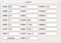
Going back to your OnSemi App Note,
I have had a go at putting the equations into a FreePascal/Lazarus application. It's not pretty but... Attached.
The results do not exactly agree with the App Note but, assuming its equations are right, look at EQ27-29. Their calculations are wrong.
Also have a look at Page 15)
Also notice that some of the equations in the OnSemi App Note include the number 8. I am used to dealing with voltage fed square wave converters whereby minimum primary turns kind of work out to be,
NPmin = VIN.TON/Bpeak.Ae
It's the integral volt-seconds applied to the primary. When you see 8 then someone is looking at a sinusoidal voltage drive rather than a square wave voltage drive. The sums are a bit incestuous but there may be another way of working things out...
You mentioned a flyback converter and that might be worth pursuing.
Later.
I have had a go at putting the equations into a FreePascal/Lazarus application. It's not pretty but... Attached.
The results do not exactly agree with the App Note but, assuming its equations are right, look at EQ27-29. Their calculations are wrong.
Also have a look at Page 15)
I think that might be fairly telling. Look back at my previous post and the Notes by Lloyd Dixon where he explains how to position/associate the Leakage Inductance with a particular winding and also estimate its value.The difference between the LLC design with external
resonant inductance and the design that uses a transformer
with high leakage inductance can be determined with
simulations. The integrated resonant tank gain differs from
the inversed transformer turns ratio when operated in series
resonant frequency. This phenomenon is related to the fact
that the leakage inductance is physically not located in series with the primary winding like in the external resonant coil solution.
Also notice that some of the equations in the OnSemi App Note include the number 8. I am used to dealing with voltage fed square wave converters whereby minimum primary turns kind of work out to be,
NPmin = VIN.TON/Bpeak.Ae
It's the integral volt-seconds applied to the primary. When you see 8 then someone is looking at a sinusoidal voltage drive rather than a square wave voltage drive. The sums are a bit incestuous but there may be another way of working things out...
You mentioned a flyback converter and that might be worth pursuing.
Later.
Attachments
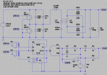
OK... So I mess about with my LTSpice model.
Again copy and save as an .asc file then open with LTSpice. I have transferred the values from my, broken, program, into it.
Right click on bits. In particular the MODULATOR, A1, is set for
Mark=160K Space=220K
B1 turns its output into digital things
V=7.5+7.5*SGN(V(PMOD))
The DFLOP, A2, does a divide by two to give FMIN/FMAX as 80K and 110K.
BUFFER, A3, in association with XOR, A4, gives the dead time
VHigh=15V Vlow=0V Td=350n
U1 is the 'error amplifier'. It's output is clamped by ZID. The compensation is 'rubbish'.
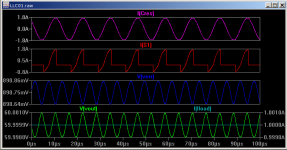
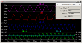
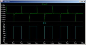
Two pictures. 1A Load and 8A Load. Yes... it appears to work but you might like to make its life harder and it will fall to pieces.
The 8A Load includes the Resonant Capacitor current. 3A RMS. The program based on the APP Note sums suggested 2.8A RMS. The sums are 'approximate' but as a check for rationality it seems things are close enough.
Code:
Version 4
SHEET 1 1176 1080
WIRE -64 32 -416 32
WIRE 16 32 -64 32
WIRE 112 32 16 32
WIRE 272 32 240 32
WIRE 384 32 352 32
WIRE 544 32 464 32
WIRE 704 32 608 32
WIRE 816 32 704 32
WIRE 944 32 816 32
WIRE 976 32 944 32
WIRE -64 96 -64 32
WIRE 16 96 16 32
WIRE 112 96 112 32
WIRE -112 112 -192 112
WIRE 464 112 464 32
WIRE 544 112 464 112
WIRE 640 112 608 112
WIRE 816 112 816 32
WIRE 384 144 384 32
WIRE 464 144 464 112
WIRE -112 160 -160 160
WIRE -416 192 -416 32
WIRE -64 224 -64 176
WIRE 16 224 16 160
WIRE 16 224 -64 224
WIRE 112 224 112 160
WIRE 112 224 16 224
WIRE 240 224 240 32
WIRE 240 224 112 224
WIRE 384 256 384 224
WIRE 464 256 464 224
WIRE 544 256 464 256
WIRE 640 256 640 112
WIRE 640 256 608 256
WIRE 816 256 816 192
WIRE 944 256 944 32
WIRE -64 272 -64 224
WIRE 16 272 16 224
WIRE 112 272 112 224
WIRE -112 288 -192 288
WIRE -160 336 -160 160
WIRE -112 336 -160 336
WIRE 464 336 464 256
WIRE 544 336 464 336
WIRE 704 336 704 32
WIRE 704 336 608 336
WIRE -416 400 -416 272
WIRE -160 400 -160 336
WIRE -160 400 -416 400
WIRE -64 400 -64 352
WIRE -64 400 -160 400
WIRE 16 400 16 336
WIRE 16 400 -64 400
WIRE 112 400 112 336
WIRE 112 400 16 400
WIRE 384 400 384 320
WIRE 384 400 112 400
WIRE 640 400 640 256
WIRE 640 400 384 400
WIRE 816 400 816 320
WIRE 816 400 640 400
WIRE 944 400 944 336
WIRE 944 400 816 400
WIRE -416 432 -416 400
WIRE 64 496 -176 496
WIRE -208 528 -240 528
WIRE 416 528 352 528
WIRE 448 528 416 528
WIRE 544 528 512 528
WIRE 656 528 624 528
WIRE 720 528 688 528
WIRE 976 528 800 528
WIRE -304 544 -336 544
WIRE -208 544 -208 528
WIRE -208 544 -240 544
WIRE -208 560 -208 544
WIRE -208 560 -240 560
WIRE 208 560 176 560
WIRE -208 576 -208 560
WIRE -208 576 -240 576
WIRE -128 592 -240 592
WIRE 64 592 64 496
WIRE 64 592 32 592
WIRE 208 592 176 592
WIRE 384 592 352 592
WIRE -176 640 -176 496
WIRE -176 640 -240 640
WIRE -144 640 -176 640
WIRE 96 640 32 640
WIRE 208 640 208 592
WIRE 208 640 96 640
WIRE 416 640 416 528
WIRE 448 640 416 640
WIRE 656 640 656 528
WIRE 656 640 512 640
WIRE 688 640 688 528
WIRE 720 640 688 640
WIRE 832 640 800 640
WIRE 944 640 912 640
WIRE -304 656 -336 656
WIRE -208 656 -208 576
WIRE -208 656 -240 656
WIRE -208 672 -208 656
WIRE -208 672 -240 672
WIRE -208 688 -208 672
WIRE -208 688 -240 688
WIRE -208 704 -208 688
WIRE -208 704 -240 704
WIRE 656 704 656 640
WIRE 656 704 624 704
WIRE 688 704 688 640
WIRE 688 704 656 704
WIRE 416 720 416 640
WIRE 560 720 416 720
WIRE 64 736 64 592
WIRE 64 736 -96 736
WIRE 656 736 624 736
WIRE -160 752 -336 752
WIRE 416 768 416 720
WIRE 448 768 416 768
WIRE -208 784 -208 704
WIRE -208 784 -336 784
WIRE -176 784 -208 784
WIRE -64 800 -96 800
WIRE 64 800 64 736
WIRE 64 800 0 800
WIRE 96 800 96 640
WIRE -128 912 -128 800
WIRE 0 912 0 816
WIRE 0 912 -128 912
WIRE 32 912 32 688
WIRE 32 912 0 912
WIRE 96 912 96 880
WIRE 96 912 32 912
WIRE 352 912 352 624
WIRE 352 912 96 912
WIRE 384 912 384 592
WIRE 384 912 352 912
WIRE 656 912 656 736
WIRE 656 912 384 912
WIRE 944 912 944 640
WIRE 944 912 656 912
WIRE 944 944 944 912
FLAG -416 432 0
FLAG 976 32 VOUT
IOPIN 976 32 Out
FLAG -192 112 DRVA
IOPIN -192 112 In
FLAG -192 288 DRVB
IOPIN -192 288 In
FLAG 976 528 VOUT
IOPIN 976 528 In
FLAG 448 768 VERR
IOPIN 448 768 Out
FLAG 944 944 0
FLAG -48 544 0
FLAG -48 688 0
FLAG -336 544 DRVA
IOPIN -336 544 Out
FLAG -336 656 DRVB
IOPIN -336 656 Out
FLAG -256 592 0
FLAG -256 704 0
FLAG 176 560 PMOD
IOPIN 176 560 Out
FLAG 176 592 DMOD
IOPIN 176 592 Out
FLAG -336 784 B
IOPIN -336 784 Out
FLAG -336 752 A
IOPIN -336 752 Out
SYMBOL ind2 368 128 R0
WINDOW 0 -64 44 Left 2
WINDOW 3 -65 70 Left 2
SYMATTR InstName LP
SYMATTR Value 340µ
SYMATTR Type ind
SYMBOL ind 256 48 R270
WINDOW 0 59 60 VTop 2
WINDOW 3 62 59 VBottom 2
SYMATTR InstName LLeak
SYMATTR Value 62µ
SYMBOL cap 368 256 R0
WINDOW 0 -65 12 Left 2
WINDOW 3 -66 37 Left 2
SYMATTR InstName CRes
SYMATTR Value 62n
SYMBOL ind2 480 240 R180
WINDOW 0 -45 68 Left 2
WINDOW 3 -56 43 Left 2
SYMATTR InstName LS
SYMATTR Value 32µ
SYMATTR Type ind
SYMBOL diode 544 48 R270
WINDOW 0 32 32 VTop 2
WINDOW 3 0 32 VBottom 2
SYMATTR InstName DR1
SYMATTR Value DID
SYMBOL diode 608 96 R90
WINDOW 0 0 32 VBottom 2
WINDOW 3 32 32 VTop 2
SYMATTR InstName DR2
SYMATTR Value DID
SYMBOL diode 608 240 R90
WINDOW 0 0 32 VBottom 2
WINDOW 3 32 32 VTop 2
SYMATTR InstName DR3
SYMATTR Value DID
SYMBOL diode 544 352 R270
WINDOW 0 32 32 VTop 2
WINDOW 3 0 32 VBottom 2
SYMATTR InstName DR4
SYMATTR Value DID
SYMBOL cap 800 256 R0
WINDOW 0 38 20 Left 2
WINDOW 3 38 49 Left 2
SYMATTR InstName CFA
SYMATTR Value 1000µ
SYMBOL sw -64 192 M180
WINDOW 0 -78 122 Left 2
WINDOW 3 -77 97 Left 2
SYMATTR InstName S1
SYMATTR Value MSW
SYMBOL sw -64 368 M180
WINDOW 0 -75 129 Left 2
WINDOW 3 -75 103 Left 2
SYMATTR InstName S2
SYMATTR Value MSW
SYMBOL diode 32 160 R180
WINDOW 0 -57 43 Left 2
WINDOW 3 -49 21 Left 2
SYMATTR InstName DB1
SYMATTR Value DID
SYMBOL diode 32 336 R180
WINDOW 0 -57 46 Left 2
WINDOW 3 -50 22 Left 2
SYMATTR InstName DB2
SYMATTR Value DID
SYMBOL cap 96 96 R0
WINDOW 0 39 19 Left 2
WINDOW 3 40 45 Left 2
SYMATTR InstName CP1
SYMATTR Value 470p
SYMBOL cap 96 272 R0
WINDOW 0 36 18 Left 2
WINDOW 3 38 43 Left 2
SYMATTR InstName CP2
SYMATTR Value 470p
SYMBOL voltage -416 176 R0
WINDOW 0 36 43 Left 2
WINDOW 3 38 69 Left 2
SYMATTR InstName VBUS
SYMATTR Value 395V
SYMBOL Opamps\\opamp 592 656 M0
WINDOW 0 9 95 Left 2
SYMATTR InstName U1
SYMBOL voltage 816 640 R270
WINDOW 0 32 56 VTop 2
WINDOW 3 -32 56 VBottom 2
WINDOW 123 0 0 Left 2
WINDOW 39 0 0 Left 2
SYMATTR InstName VRef
SYMATTR Value -6
SYMBOL res 816 512 R90
WINDOW 0 0 56 VBottom 2
WINDOW 3 32 56 VTop 2
SYMATTR InstName R2
SYMATTR Value 100K
SYMBOL res 640 512 R90
WINDOW 0 0 56 VBottom 2
WINDOW 3 32 56 VTop 2
SYMATTR InstName R3
SYMATTR Value 10K
SYMBOL res 704 656 R270
WINDOW 0 32 56 VTop 2
WINDOW 3 0 56 VBottom 2
SYMATTR InstName R4
SYMATTR Value 10K
SYMBOL SpecialFunctions\\modulate 352 528 M0
SYMATTR InstName A1
SYMATTR SpiceLine Mark=160K Space=220K
SYMBOL Digital\\dflop -48 544 M0
WINDOW 0 48 -19 Left 2
SYMATTR InstName A2
SYMATTR SpiceLine Vhigh=15V Vlow=0V
SYMBOL Digital\\and -272 496 M0
SYMATTR InstName A5
SYMATTR SpiceLine Vhigh=15V Vlow=0V
SYMBOL Digital\\and -272 608 M0
SYMATTR InstName A6
SYMATTR SpiceLine Vhigh=15V Vlow=0V
SYMBOL Digital\\xor -144 704 M0
SYMATTR InstName A4
SYMATTR SpiceLine Vhigh=15V Vlow=0V
SYMBOL diode 512 624 R90
WINDOW 0 0 32 VBottom 2
WINDOW 3 32 32 VTop 2
SYMATTR InstName ZD1
SYMATTR Value ZID
SYMBOL Digital\\buf1 0 736 M0
SYMATTR InstName A3
SYMATTR SpiceLine VHigh=15V Vlow=0V Td=350n
SYMBOL bv 96 784 R0
WINDOW 0 46 54 Left 2
WINDOW 3 24 96 Invisible 2
SYMATTR InstName B1
SYMATTR Value V=7.5+7.5*SGN(V(PMOD))
SYMBOL res 800 96 R0
SYMATTR InstName RESR
SYMATTR Value 1p
SYMBOL current 944 256 R0
WINDOW 0 40 34 Left 2
WINDOW 3 24 80 Invisible 2
WINDOW 123 0 0 Left 2
WINDOW 39 0 0 Left 2
SYMATTR InstName ILOAD
SYMATTR Value PULSE(8 8 0 100n 100n 1m 2m)
SYMBOL cap 512 512 R90
WINDOW 0 0 32 VBottom 2
WINDOW 3 32 32 VTop 2
SYMATTR InstName C1
SYMATTR Value 100n
TEXT -424 928 Left 2 !K1 LP LS 1
TEXT -424 976 Left 2 !.MODEL DID D(Ron=10m Roff=1E7)
TEXT -424 952 Left 2 !.MODEL MSW SW(Ron=10m Roff=1E7 Vt=7V5)
TEXT -424 1024 Left 2 !.LIB OPAMP.SUB
TEXT -424 1048 Left 2 !.tran 0 50.1m 50m 10n uic
TEXT -424 1000 Left 2 !.MODEL ZID D(Ron=10m Roff=1E9 VRev=1V)
LINE Normal 416 224 416 144 2
LINE Normal 432 224 432 144 2
Again copy and save as an .asc file then open with LTSpice. I have transferred the values from my, broken, program, into it.
Right click on bits. In particular the MODULATOR, A1, is set for
Mark=160K Space=220K
B1 turns its output into digital things
V=7.5+7.5*SGN(V(PMOD))
The DFLOP, A2, does a divide by two to give FMIN/FMAX as 80K and 110K.
BUFFER, A3, in association with XOR, A4, gives the dead time
VHigh=15V Vlow=0V Td=350n
U1 is the 'error amplifier'. It's output is clamped by ZID. The compensation is 'rubbish'.
Two pictures. 1A Load and 8A Load. Yes... it appears to work but you might like to make its life harder and it will fall to pieces.
The 8A Load includes the Resonant Capacitor current. 3A RMS. The program based on the APP Note sums suggested 2.8A RMS. The sums are 'approximate' but as a check for rationality it seems things are close enough.
Attachments
Thanks a lot for taking the time to do this!
I tried to load the file in LTSPice and it works. You have great skills in simulating.
One interesting thing is that the voltage on primary bus will drop a lot if the mains voltage is low and the mains cap is small. I measured down to 200V in my test-setup. That drives the primary-current up if output regulation is to be maintained.
I think that the next step with the current prototype is to verify whether the primary current actually rises above the saturation-limit or if I have another limitation somewhere.
TroelsM
Thanks a lot for taking the time to do this!
I tried to load the file in LTSPice and it works. You have great skills in simulating.
Thanks. My model still has mistakes. In particular the range I have set for the Modulator. Fmin can probably go lower. Check the OnSemi APP Note. Fnom, 395V, might be 80K but to get regulation down to 350V you have to set a lower value for the Modulator. Try their linear model to see how far down you can go before you hit Non-ZVS... drop of the left side of the peak. Again my compensation scheme is rubbish.
I should say Thank You for pointing me at that particular application note. I have looked at these things in the past and got nowhere.
In respect of Spice, for me, KISS works, especially for SMPS. Use the simplest bits to approximate what you have so you can have a chance to see what might be going on without hitting non-convergence errors in A when the problem was in Z. Sometimes you still have to tweak A a bit.
One interesting thing is that the voltage on primary bus will drop a lot if the mains voltage is low and the mains cap is small. I measured down to 200V in my test-setup. That drives the primary-current up if output regulation is to be maintained.
Stuff like that happens. You should really check it out.
Your input bulk capacitor will charge up to 1.14 x RMS input voltage. Then it discharges as your power supply sucks current out of it. If you assume a constant current then dV/dT = i/C over 50mS if you are at 50Hz. Something like that.
Google/Wikipedia?
I think that the next step with the current prototype is to verify whether the primary current actually rises above the saturation-limit or if I have another limitation somewhere.
TroelsM
The OnSemi APP Note gives you a sum to estimate your minimum primary turns. I went off in a box elsewhere but it assumes a sinusoidal voltage drive and that would appear to be valid.
Flux excursion is integral of volt-seconds. Typical ferrites can be operated up to 300mT. Look at the Siemens/EPCOS data sheets. In this sort of converter, other than under transient conditions, the flux excursion is symmetrical about 0 so your base figure, dB, might be 600mT, +/-300mT.
It's reduced because you run into Core Loss Limitations. Again the Siemens/EPCOS data sheets give you graphs... of Pv/m^3 for various operating frequencies and, half, flux excursions. You also get tables for various cores giving thermal impedance for passive cooling fully wound.
Seriously... Rather than using a bit of junk from an old ATX supply. Think about dropping some money on your local electronics supplier to buy something you can design with.
Just for the fun of it I went overboard. LCC resonant. 350 in 60V out. 1A/8A transient. You will not get to know. Meh.
Attachments
Found another app-note that deals with the transformer in a different way.
Page 12:
http://www.ti.com/lit/ug/slou293c/slou293c.pdf
I (think I), understand why this winding-scheme can give a "better" inductance-ratio, but for DIY it looks more complicated with regards to materials and safety-distances.
Kind regards TroelsM
Page 12:
http://www.ti.com/lit/ug/slou293c/slou293c.pdf
I (think I), understand why this winding-scheme can give a "better" inductance-ratio, but for DIY it looks more complicated with regards to materials and safety-distances.
Kind regards TroelsM
Another excellent find.. .
http://www.ti.com/lit/ug/slou293c/slou293c.pdf
don't forget...
http://www.ti.com/lit/ml/slup105/slup105.pdf
Where Lloyd Dixon, formerly of Unitrode which was bought up by TI, describes and characterises the same technique.
Possibly one thing to note is, once again, where the leakage inductance is located within the transformer/inductor. In the older note it is associated with the outer winding, L1. In the newer document it will again be associated with the outer winding. In this case the secondary windings.
The OnSemi application note mentions that the basic analysis depends on the leakage inductance being associated with the primary. It does go on to propose how the result might be adapted for 'another' case. However I'm not certain how precise or valid the proposal might be. Especially if there is uncertainty as to where the leakage inductance is in fact located.
I have always had some difficulty visualising the actual structure of these things but, and I will probably be wrong, it is not possible to model such things reliably in SPICE using coupled inductors... As a result I would be inclined to follow the method proposed by Dixon and associate the leakage inductance with the Primary. Swap the order given in the newer note with secondaries internal and primary external.
Of course as per the OnSemi note it may be possible to make adjustments. Otherwise you are back into the realms of 'suck it and see', 'cut and try'. Ultimately using the method as described, but swap the winding order, appears to give you the best possibility of designing something that will behave in the way you have designed it.
This may not make the most 'efficient' use of the core or, in particular, winding area but things will remain in a 'comfort zone'. It may be the case that for volume manufacturing it will be worthwhile to shave costs by playing dirty but you may invite hidden consequences. It would appear that most hobbyists end up scratching their heads when things do not work as expected whilst others could claim working solutions but, other than 'look it works', might not be able to claim that the underlying design is robust.
It is not so much that the actual method gives a better inductance ratio. More importantly it gives a relatively predictable and calculable inductance and inductance ratio... perhaps +/-10%. If you want to play dirty then you might achieve better for the same core/bobbin for various definitions of better.
In respect of DIY and in particular Agency Requirements it may 'look' more complicated. In respect of volume manufacturing it is all much of a muchness. Either way there are more than a few ways to simplify your design. The major one for a hobbyist will be the use of triple insulated wire, TEX-E
In the TI design they mention 3.2mm spacers. This is for creepage/clearance of 6mm and would, in old days, have been implemented using 'margin tape'. With TEX-E the 'problem' goes away.
Also the TI design uses one row of pins for primary terminations and the other row of pins for secondary terminations. Again this is for isolation.
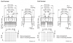
I have attached a picture of an ETD39 bobbin, as used in the TI example. Left is Original and Right is Modified. Pin spacing is 5.08mm. By chopping out two of the pins I have achieved in excess of the required 6mm creepage/clearance distances.
Basically you aim to terminate/wind/terminate from one side of the bobbin to the other side with no returns and connect on the board. Two Primaries, 4 pins. One Primary Auxiliary, 2 pins. Two Secondaries, 4 pins. Two Secondary Auxiliaries, 4 pins.
TEX-E for the primaries and auxiliaries. As you have previously noted you might wish to associate the auxiliaries with the secondaries for the purpose of regulation. The TEX-E lets you do that, in particular for the primary one, without having to worry too much about isolation requirements.
Other logistics may or may not apply. The trick is to consider the possibilities based on what you have available and work to keep things neat... otherwise place the lumps where they have less impact.
http://www.ti.com/lit/ug/slou293c/slou293c.pdf
don't forget...
http://www.ti.com/lit/ml/slup105/slup105.pdf
Where Lloyd Dixon, formerly of Unitrode which was bought up by TI, describes and characterises the same technique.
Possibly one thing to note is, once again, where the leakage inductance is located within the transformer/inductor. In the older note it is associated with the outer winding, L1. In the newer document it will again be associated with the outer winding. In this case the secondary windings.
The OnSemi application note mentions that the basic analysis depends on the leakage inductance being associated with the primary. It does go on to propose how the result might be adapted for 'another' case. However I'm not certain how precise or valid the proposal might be. Especially if there is uncertainty as to where the leakage inductance is in fact located.
I have always had some difficulty visualising the actual structure of these things but, and I will probably be wrong, it is not possible to model such things reliably in SPICE using coupled inductors... As a result I would be inclined to follow the method proposed by Dixon and associate the leakage inductance with the Primary. Swap the order given in the newer note with secondaries internal and primary external.
Of course as per the OnSemi note it may be possible to make adjustments. Otherwise you are back into the realms of 'suck it and see', 'cut and try'. Ultimately using the method as described, but swap the winding order, appears to give you the best possibility of designing something that will behave in the way you have designed it.
This may not make the most 'efficient' use of the core or, in particular, winding area but things will remain in a 'comfort zone'. It may be the case that for volume manufacturing it will be worthwhile to shave costs by playing dirty but you may invite hidden consequences. It would appear that most hobbyists end up scratching their heads when things do not work as expected whilst others could claim working solutions but, other than 'look it works', might not be able to claim that the underlying design is robust.
It is not so much that the actual method gives a better inductance ratio. More importantly it gives a relatively predictable and calculable inductance and inductance ratio... perhaps +/-10%. If you want to play dirty then you might achieve better for the same core/bobbin for various definitions of better.
In respect of DIY and in particular Agency Requirements it may 'look' more complicated. In respect of volume manufacturing it is all much of a muchness. Either way there are more than a few ways to simplify your design. The major one for a hobbyist will be the use of triple insulated wire, TEX-E
In the TI design they mention 3.2mm spacers. This is for creepage/clearance of 6mm and would, in old days, have been implemented using 'margin tape'. With TEX-E the 'problem' goes away.
Also the TI design uses one row of pins for primary terminations and the other row of pins for secondary terminations. Again this is for isolation.
I have attached a picture of an ETD39 bobbin, as used in the TI example. Left is Original and Right is Modified. Pin spacing is 5.08mm. By chopping out two of the pins I have achieved in excess of the required 6mm creepage/clearance distances.
Basically you aim to terminate/wind/terminate from one side of the bobbin to the other side with no returns and connect on the board. Two Primaries, 4 pins. One Primary Auxiliary, 2 pins. Two Secondaries, 4 pins. Two Secondary Auxiliaries, 4 pins.
TEX-E for the primaries and auxiliaries. As you have previously noted you might wish to associate the auxiliaries with the secondaries for the purpose of regulation. The TEX-E lets you do that, in particular for the primary one, without having to worry too much about isolation requirements.
Other logistics may or may not apply. The trick is to consider the possibilities based on what you have available and work to keep things neat... otherwise place the lumps where they have less impact.
Attachments
Hi.
As for the 6mm spacing: I have disassembled a lot of ATX-transformers (NOT LLC) and quite a lot of "winding-volume" is wasted in these due to the "spacing-tape" that is used in the end of each winding to get the creepage/clearance.
On the other hand when I see pictures of commercially available LLC smps for audio there is no sign of this spacing-tape, the windings are often side-by-side, and apparently they get the creepage/clearance just with the transformer-bobbin having the spacing and grooves placed strategically.
This is one of the things that attracted me about LLC: the option for huge creepage/clearance with relatively simple and diy-friendly things.
99% of all ATX-transformers have vertical center-leg and the ETD39 you show have the centerleg horizontally. The latter option are probably preferable as the terminations of pri and sec goes to opposite sides of the bobbin.
As for why to this for diy: certainly not for the money. The complete 500W LLC units are pretty cheap, and compared to the time/cost of making just a simple working LLC-prototype the diy-rute is ONLY for the fun (and the challenge") )
)
Kind regards TroelsM
As for the 6mm spacing: I have disassembled a lot of ATX-transformers (NOT LLC) and quite a lot of "winding-volume" is wasted in these due to the "spacing-tape" that is used in the end of each winding to get the creepage/clearance.
On the other hand when I see pictures of commercially available LLC smps for audio there is no sign of this spacing-tape, the windings are often side-by-side, and apparently they get the creepage/clearance just with the transformer-bobbin having the spacing and grooves placed strategically.
This is one of the things that attracted me about LLC: the option for huge creepage/clearance with relatively simple and diy-friendly things.
99% of all ATX-transformers have vertical center-leg and the ETD39 you show have the centerleg horizontally. The latter option are probably preferable as the terminations of pri and sec goes to opposite sides of the bobbin.
As for why to this for diy: certainly not for the money. The complete 500W LLC units are pretty cheap, and compared to the time/cost of making just a simple working LLC-prototype the diy-rute is ONLY for the fun (and the challenge
)Kind regards TroelsM
Last edited:
agreed.Hi.
As for the 6mm spacing: I have disassembled a lot of ATX-transformers (NOT LLC) and quite a lot of "winding-volume" is wasted in these due to the "spacing-tape" that is used in the end of each winding to get the creepage/clearance.
On the other hand when I see pictures of commercially available LLC smps for audio there is no sign of this spacing-tape, the windings are often side-by-side, and apparently they get the creepage/clearance just with the transformer-bobbin having the spacing and grooves placed strategically.
This is one of the things that attracted me about LLC: the option for huge creepage/clearance with relatively simple and diy-friendly things.
99% of all ATX-transformers have vertical center-leg and the ETD39 you show have the centerleg horizontally. The latter option are probably preferable as the terminations of pri and sec goes to opposite sides of the bobbin.
As for why to this for diy: certainly not for the money. The complete 500W LLC units are pretty cheap, and compared to the time/cost of making just a simple working LLC-prototype the diy-rute is ONLY for the fun (and the challenge
Kind regards TroelsM
To answer an old question: The resonant frequency of LLC circuit is constant and independent of load.
The q-factor varies with load.
And yes, I use special sectional bobbins as you described above.
Concerning catastrophic turn-on failures:
At the first moment the secondary is shorted by the bulk caps.
To avoid excessing primary current flow, the clock frequency should start far above series resonant frequency.
Most controllers provide a softstart feature to accomplish this.
Be aware that without a current limiting, short circuit at a clock frequency close to series resonant frequency will blow any primäry MOSFET - this is the well known resonant catastrophic case.
The LLC is per se NOT short circuit proof.
There are cycle-by-cycle overcurrent protection features implemented in various controller chips, I cannot comment on these.
My preferred current limiting solution are 2 diodes clamping primary resonant voltage to the power rails. This has proven rock solid in practical applications and does not require a soft start.
- Home
- Amplifiers
- Power Supplies
- Power limitations for LLC-smps for amplifier