Keep the caps and their traces as close as possible to the chip, the 100nF being closest. Connect their 0V together and then back to the power supply. This will hopefully make grounding clearer for you http://hifisonix.com/wordpress/wp-c...re-up-a-Power-Amplifier_Updated-Autosaved.pdf
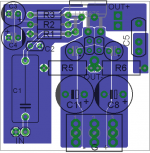
Here is what I did so far. I honestly don't know what I'm doing (at least for now). I hope someone could lay an example on my layout if its not too much to ask


that was in english.Uhmm... English please... haha lol. I really don't understand what you said. As I said I'm a novice in this thing.
When you said "split", did you mean I have traces of GND from the amps side at one point and then another traces of GND at the power supply at one different point? Is it just safe to put a one whole ground plane on the entire PCB? I am completely no idea. If you could lay it out for me, I will really appreciate that.
What is your native language?
You have no information in your profile.
Now back to my post and your remark.
What parts do you not understand?
Give a specific question for each part.
that was in english.
What is your native language?
You have no information in your profile.
Now back to my post and your remark.
What parts do you not understand?
Give a specific question for each part.
I know it was in english. What I'm trying to emphasize is say it to me where I can understand it easily, not in technical terms. As I said, I am a novice in this thing but I want to learn. Anyway, I really appreciate your input and thank you for that.

Or maybe you can make an example on the layout that I made, if its not too much to ask
When laying out grounds there are two questions you must always keep in mind:
1. Where do the currents flow? They always flow in loops, and they always develop voltage drops along their route.
2. What is the reference point for each 'voltage'? Voltages are always between two points, so you need to ensure that what you think is the signal is the same as what the circuit thinks is the signal.
Your circuit ground connection should be taken from the clean side of the trace from the secondary CT to the reservoir capacitor junction. At present you have it on the dirty side, which means a little extra buzz on the supply rails. The order should be CT - caps - circuit.
Here is what I did so far. I honestly don't know what I'm doing (at least for now). I hope someone could lay an example on my layout if its not too much to ask
It looks like you are trying to create a "T" 0V connection, but you have the returns in the wrong order, have another look at the "T" in the pictures towards the end of the doc I linked. All of the signal returns(0V) should be kept physically close to their counterpart sends, treat them as a pair, see on the link how the speaker return is connected for example
Here is a layout that I made last year. I wanted to see if it was possible to layout a single sided board for this chip.
It also demonstrates what AndrewT is explaining about flow and return. Trace the input signal path from IN-C1-R1 back to IN via the ground plane.
It also demonstrates what AndrewT is explaining about flow and return. Trace the input signal path from IN-C1-R1 back to IN via the ground plane.
Attachments
It looks like you are trying to create a "T" 0V connection, but you have the returns in the wrong order
Am I getting closer to doing it right? haha
Here is a layout that I made last year. I wanted to see if it was possible to layout a single sided board for this chip.
It also demonstrates what AndrewT is explaining about flow and return. Trace the input signal path from IN-C1-R1 back to IN via the ground plane.
Thanks Mark, I think I slowly grasping the idea.
Your circuit ground connection should be taken from the clean side of the trace from the secondary CT to the reservoir capacitor junction. At present you have it on the dirty side, which means a little extra buzz on the supply rails. The order should be CT - caps - circuit.
Duly noted, sir.
As I understand, the return path for my left input are C2, C3 and R2. For my left ouput is R6. For My Right Input are C20, C21 and R12. For my Right output is R16.
Here it is guys from what I understand on what you guys are trying to tell me.

Last edited:
Can we forget the right channel amp for a moment, you have the same layout so it would be best to take your 0V back to the PSU by a more direct route. Also the returns on the right channel are still in the wrong order. If you break the track between the signal GND and 0V you will be able to add a hum breaking resistor (HBR) if necessary, this is R5 in Mark's layout

You seem to have gone back to a kind of star?
Is it bad? How close I am to getting it right?
The ideal way would be like on page 21 here http://hifisonix.com/wordpress/wp-c...re-up-a-Power-Amplifier_Updated-Autosaved.pdf which is also how Mark did it on his layout. The speaker return is connected to the decoupling capacitors and the signal (and feedback) return is connected to the same point via the hum breaking resistor (HBR), this 0V is then take back to the main T at the power supply capacitors
loop area rules.
That is what leads to the rule of:
close coupled pair for the signal wires.
You must identify the signal flow route and you as layout technician must ensure that the return route follows the flow route as closely as possible.
You must do that for every signal pair.
That is what leads to the rule of:
close coupled pair for the signal wires.
You must identify the signal flow route and you as layout technician must ensure that the return route follows the flow route as closely as possible.
You must do that for every signal pair.
- Status
- This old topic is closed. If you want to reopen this topic, contact a moderator using the "Report Post" button.
- Home
- Amplifiers
- Power Supplies
- 2 Separate Transformers