Hi,
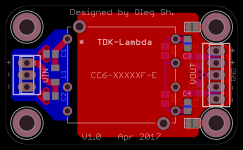
Inspired by the success of several diyaudio members in using switching power PSUs for audio applications I decided to give it a try. The idea is to use a simple USB charger to power a pre- or a head-amp. This requires using the DC-DC converter to get a bipolar supply out of a single 5VDC supply. Since I am not yet skilled in laying out PCBs for such delicate circuits like switching converters I decided to start with the ready made solution. I screened several possible candidates and decide to give a try to TDK-Lambda converters first. I tested the CC6-0512DF-E converter on the bread board. The result is posted in my head-amp design thread. I find it not conclusive since I am not sure that I measure the converter input and output correctly. Plus it lacks external input and output filters which are recommended by the manufacturer to further reduce the ripple. Using through-hole parts for the filter did not change anything in my tests so I assume I should use SMD parts to reduce parasitic coupling of the noise.
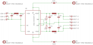
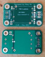
Attached is the schematic and a simple PCB design with input and output Pi filters and output voltage trimming resistors as suggested by the manufacturer. The PCB should simplify the testing and help to reduce the output ripple should there be a problem with it.
Parts:
C1, C2 = 10uF (0805 X7R)
C3 - C6 = 1uF (0805 X7R)
L1 = 1206 ferrite bead 600Ohm @ 100MHz, 2.5 A
L2, L3 = 1206 ferrite bead 1kOhm @100MHz, 1 A
The metal case of the DC-DC converter is connected to the output common (GND). I hope this should reduce radiated noise inside the chassis. The input of the converter is galvanically isolated from the output and I made it floating. This should help to keep the ground noise coming from the USB charger away from the downstream circuit and also avoid ground loops. The GND plane of the PCB can be connected to chassis via the metal standoffs/spacers using solder jumpers.
I would appreciate any comments on the PCB design especially if someone sees obvious or not so obvious potential problems with it.
Regards,
Oleg
Inspired by the success of several diyaudio members in using switching power PSUs for audio applications I decided to give it a try. The idea is to use a simple USB charger to power a pre- or a head-amp. This requires using the DC-DC converter to get a bipolar supply out of a single 5VDC supply. Since I am not yet skilled in laying out PCBs for such delicate circuits like switching converters I decided to start with the ready made solution. I screened several possible candidates and decide to give a try to TDK-Lambda converters first. I tested the CC6-0512DF-E converter on the bread board. The result is posted in my head-amp design thread. I find it not conclusive since I am not sure that I measure the converter input and output correctly. Plus it lacks external input and output filters which are recommended by the manufacturer to further reduce the ripple. Using through-hole parts for the filter did not change anything in my tests so I assume I should use SMD parts to reduce parasitic coupling of the noise.
Attached is the schematic and a simple PCB design with input and output Pi filters and output voltage trimming resistors as suggested by the manufacturer. The PCB should simplify the testing and help to reduce the output ripple should there be a problem with it.
Parts:
C1, C2 = 10uF (0805 X7R)
C3 - C6 = 1uF (0805 X7R)
L1 = 1206 ferrite bead 600Ohm @ 100MHz, 2.5 A
L2, L3 = 1206 ferrite bead 1kOhm @100MHz, 1 A
The metal case of the DC-DC converter is connected to the output common (GND). I hope this should reduce radiated noise inside the chassis. The input of the converter is galvanically isolated from the output and I made it floating. This should help to keep the ground noise coming from the USB charger away from the downstream circuit and also avoid ground loops. The GND plane of the PCB can be connected to chassis via the metal standoffs/spacers using solder jumpers.
I would appreciate any comments on the PCB design especially if someone sees obvious or not so obvious potential problems with it.
Regards,
Oleg
Attachments
Last edited:
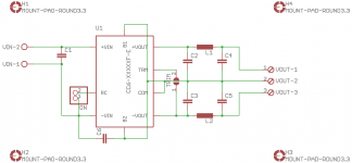
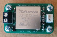
PCBs arrived. I've slightly simplified the input side of the converter (see attached schematic). I assembled one unit and will do some testing today or tomorrow.
Attachments
Hi Oleg, did you consider placing the bypass caps on the rear (ie. directly located between dc/dc package pins) to minimise the length taken for the current path through each cap?
What value bypass caps are you planning on trying - you have only allowed yourself one capacitor pad per bypass, although there seems to be room for a lot more.
The output terminal gnd (quiet end) of the pi filter seems to be blended in to the common gnd at the converter as you've used a flood plane.
Did you consider what options were available to extend the module case through to the pcb and under the module, but as a screen, compared to just an output 0V flood?
Well, I considered many possibilities but somehow decided to restrict myself to what is actually produced. Datasheet and application notes for the TDK-Lambda modules suggest a single ceramic 10uF cap bypass right at the input pin and one 1uF cap at each output. I went a bit further and used a Pi filter with ferrite bead at the outputs (2x1uF cap and one Z=1k@100MHz ferrite bead). The Pi filter at the output is not meant to filter the switching frequency ripple but to attenuate the ringing at ~100Mhz that I discovered in my measurements.
As for using the screen and GND plane as one entity has to do with the app note suggestion to experiment with the connection of the metal cage to either input negative or output common pins. I did not plan to experiment with that and decided to connect the shield to the output GND to avoid incoming noise being radiated by the shield which would happen if the shield would be connected to the input negative supply pin. I guess leaving the metal case floating is not a good idea as it will radiate all kinds of noise it will pick up from the converter during its operation. Measurements will tell if I am right on this.
As for using the screen and GND plane as one entity has to do with the app note suggestion to experiment with the connection of the metal cage to either input negative or output common pins. I did not plan to experiment with that and decided to connect the shield to the output GND to avoid incoming noise being radiated by the shield which would happen if the shield would be connected to the input negative supply pin. I guess leaving the metal case floating is not a good idea as it will radiate all kinds of noise it will pick up from the converter during its operation. Measurements will tell if I am right on this.
As for the caps being close to the pins, they are actually ~1.5mm from the pins. If placed on the underside they will be another 1.6 mm further away from the converter (pin length going through 1.6mm thick PCB). I guess 3 vias going to the GND plane for each cap have sufficiently low inductance to justify such placement.
The Pi filter suggested in the datasheet suppose to be located closer to the load and should use 100uH inductors. I plan to use LC filter after the PSU board by using leaded inductors to connect it to the load (which has some filter capacitance on board). Whether extra LC filter is necessary or not I'll check with measurements. The plan is to run an op-amp based line buffer and see if any of the PSU related issues appear at the buffer output. I also have some 100uH (300mA max DC current) inductors in 1210 package which I can use in place of the ferrite beads just to check if it makes noticeable difference. I also have some small clamp-on ferrite beads which I can clamp on the power supply wires to suppress the spikes. So a lot of experimentation is ahead")
That's interesting Oleg - are you picking the 100MHz up with an antenna and spectrum analyser?
If noise from the input supply was a concern, would it be a titch better not to flood the input neg to cover so much area, and rather just overlap top and bottom traces from the input terminals to the converter terminals?
Given a concern about 100MHz, I think Jan and I were looking at straight line path length through the bypass cap, including the straight line distance through the flood plane back to the module pin. Not having a common section of trace for the bypass cap and the inductor may also have some advantage.
That's nice. I'd be following your results. I guess one important issue is to find a way to measure what you want to measure. Short test leads, very short ground connections etc are important. It is easy to get things on the scope that are not at the intended points...
Jan
Jan
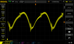
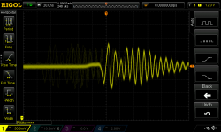
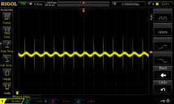
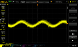
Attached are the measurements results. What is interesting is that when I measure across the output terminal I get no spike noise but more or less clean 220kHz ripple voltage of 20mVp-p. I consider such result really good since this ripple will be further reduced by the filter capacitors at the load.
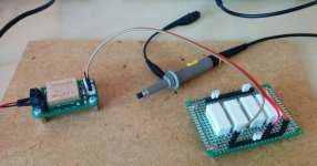
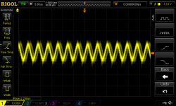
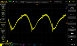
If I measure across the load with wide space between wires (see attached measurement setup picture) I pick up a lot of spike noise. The zoom-in of the spikes (ringing) is also attached.
The last image shows input ripple. I used USB battery pack to power the TDK-Lambda converter.
If I measure across the load with wide space between wires (see attached measurement setup picture) I pick up a lot of spike noise. The zoom-in of the spikes (ringing) is also attached.
The last image shows input ripple. I used USB battery pack to power the TDK-Lambda converter.
Attachments
Oleg, it's always difficult to determine whether the probed signal includes some contribution from nearby radiated fields. The standard springy grounding clip does a good job, but still presents some 'area' for coupling in to.
It appears that the primary side is the likely source of your observed 100MHz glitches. If practical, probing on C2-3, and then C4-5 may show some difference in glitch level, but that could be probing orientation just as much as the influence of the inductor.
Have you checked the ripple and noise signal from your proposed power source (USB charger), or were you only going to use that for battery charging, and use a battery during normal operation?
The Silent Switcher is IMHO a better solution.
The switcher IC itself can go up to +/-40V, so +/-24V as used for many discrete line amps or headamps is no issue.
Also the wide band regulator can clean up the HF ripple from the switcher.
(Assuming you do not need much more than 5W in total.)
We used it to power a Wurcer LNA and the output spectrum is essentially the same as batteries.
Patrick
Last edited:
Have you checked the ripple and noise signal from your proposed power source (USB charger), or were you only going to use that for battery charging, and use a battery during normal operation?
I'll repeat the measurements using USB charger that I plan to use with the DC-DC converter.
Even if the USB charger or the battery is clean on itself, these converters spew back a lot of junk to their source. That in itself can again cause EMI into the circuit that is powered.
Jan
I will repeat the input side measurements but this time probing across C1. Maybe it will show what is really going on there. My earlier measurements were across the screw terminals, so I might have picked up some radiated spike noise.
I found the exact set of ground spring clips at mouser.
I repeated converter measurements using the USB charger as power source. There is almost no change compared to the battery pack. Next is to see how good I can filter 220kHz ripple using LC filter (100uH + 100uF). According to the online calculator the ripple should be around 80dB down.
I repeated converter measurements using the USB charger as power source. There is almost no change compared to the battery pack. Next is to see how good I can filter 220kHz ripple using LC filter (100uH + 100uF). According to the online calculator the ripple should be around 80dB down.
Attachments
- Status
- This old topic is closed. If you want to reopen this topic, contact a moderator using the "Report Post" button.
- Home
- Amplifiers
- Power Supplies
- DC-DC converter based PSU for line level applications