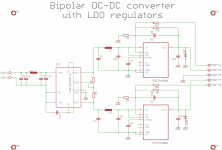
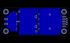
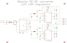
Attached is a regulated version of the DC-DC converter. I incorporated CLC input filter where L1 is a ferrite bead with ~600 Ohm impedance at 100Mhz (can be approximated as ~1uH inductor). Assuming 20uF capacitance before and after the ferrite bead in addition to reducing the spike noise/ringing it should also provide around 30dB attenuation of 220kHz input ripple (forward and reflected). The output ferrite beads (L2, L3) are 1kOhm impedance at 100MHz (around 1.5uH equivalent inductance) followed by 10uF capacitors should give around 28dB attenuation of the 220kHz ripple before the regs. Regs themselves have around 60 dB PSRR at this frequency which should bring measured 10mVp-p ripple down to uV level comparable to the overall regulator output noise. I think I'll give this design a go and compare the result with the bare DC-DC converter followed by the LC filter as mentioned in the earlier post. I am still thinking that minimalistic solution can still be sufficient but measurements will tell.
Attachments
Oleg, the incoming DC is really just a floating pair of wires with a DC level between them - the negative isn't necessarily 'gnd'. The containment of input noise/ripple may be enhanced when the neg input goes directly to the input cap terminals only, and from there to the cap terminals bypassing the dc/dc. If possible, positive and negative traces should overlay each other on either side of the pcb, to minimise any ability to radiate, and to maximise capacitance between the polarities. Flooding that gnd area only increases the capacitive coupling from dc input to your quiet dc output.
If you have a concern about very high frequency noise, then it may be worth using the pcb to continue providing the screening effect of the metal covering of the dc/dc module, but for that "screen" to just connect back to the common terminal of the output. That screen is better as the top layer of the pcb and directly underneath the module, as that is closest to the circuitry within the module. The bottom layer can be a normal 0V screen that connects to the output DC circuitry (as close to the quiet output terminal end as possible.
If you have a concern about very high frequency noise, then it may be worth using the pcb to continue providing the screening effect of the metal covering of the dc/dc module, but for that "screen" to just connect back to the common terminal of the output. That screen is better as the top layer of the pcb and directly underneath the module, as that is closest to the circuitry within the module. The bottom layer can be a normal 0V screen that connects to the output DC circuitry (as close to the quiet output terminal end as possible.
Last edited:
Hi trobbins,
Thanks for the hints! Before I start modifying the PCB design I would like to clarify few points.
Input routing:
While I agree that input wires are just that - two wires with potential difference between them, there are multiple ways to route them. If I understand it right the trace over the plane has lower inductance than a pair of traces above each other. In addition most of the parasitic inductance appears in series with the trace rather than the plane. Thus in my design most of the noise radiated by the input is coming from the short trace connecting ferrite bead to the DC-DC converter positive supply entry point. To further eliminate common mode noise the datasheet of the DC-DC converter suggests connecting 1nF ceramic capacitor between the input negative and output common terminals (I have dedicated SMD pads for this on the underside), which effectively makes input negative supply copper pour and extension of the output GND plane at high frequencies. I will experiment with this and see if it has any effect.
DC-DC converter screen connection:
In principle I agree that DC-DC converter should have a corresponding "screen" plane just beneath it (on the top layer). As for the screen connection to the "quiet" end of the output GND plane - it is not so easy to accomplish since any significant length of trace will have too high inductance to keep the potentials equal. Thus I will probably just extend the top layer GND plane to under the DC-DC converter, stitch it to the bottom GND plane with multiple vias, and stop there assuming more or less uniform reference potential of the entire output GND plane.
Please correct me if I am wrong in my assumptions.
Controlling noise is really a complex topic to work through properly - so we can but provide snippets of comments.
Most black-box related control methods are based on a specific test configuration, where noise frequencies below 30MHz get measured as conducted currents egressing the black-box, and higher frequencies are tested by antennas. Both measurement setups are complicated as they require test gear, although determining if option A or B is better can look for a relative difference, and so not need calibration, but some care is needed in trying to determine if a performance, or change is good or not.
Does it matter if noise heads back out the input wiring - well yes, if it radiates, or forms a closed current path somehow (eg. which may be via other equipment connecting to the line amp circuitry). If the line amp was operating in complete isolation (eg. wifi input, and optical fibre or isolated speaker output) then that would remove a noise path.
For a transient generated within the dc/dc, then it can egress as common mode, in which case your filtering should try to be balanced (L in each polarity) and as symmetrical a path for both polarity traces. For differential, the noise needs to be shunted from one polarity to the other as close to the dc terminals as possible.
Having a ladder style of tracing from the dc/dc terminals, to the shunt capacitor terminals, and then series L connecting to the capacitor terminals (not the dc/dc terminals), etc tries to force any noise current to take a particular path, with any voltage drop across traces from the noise current not being seen further along the 'ladder'. I'm sure there are some good tutorials/schematics on-line for this.
Even using coax, shielded or twisted pair to the dc/dc input adds shunt capacitance across the polarities, compared to separated wires.
Wrt to any screening of the dc/dc module, I agree that the screen should have a low impedance connection back to common - whether that is done at the dc/dc 0V terminal or further afield depends on practical tracing. On reflection, it may be better to close that loop at the dc/dc 0V terminal as the aim would be to return capacitive current back in to the dc/dc with as little interaction with other external circuitry.
Wrt to input to output coupling - I think that very much depends on the bigger picture of what everything connects to, and from, and what external noise requirements need to be met. I would think that minimising stray capacitive coupling from input to output of the dc/dc module is a benefit for your situation - rather than adding to it by having closely spaced large lands.
Last edited:
If this noise is suspected to be common mode would two inductors wound in anti phase on a core not reduce or cancel it? These may be used at input or output. For instance L2 and L3 may be on the same core. The input L1 could be split into two windings in antiphase on one core.
Last edited:
Thanks a lot for the comments and suggestion, trobbins!
I follow your comments but there are still some concerns which, as you mentioned, will be hard to check/prove without performing comprehensive measurements (which is not possible for me as a diyer).
I did consider using bifilar choke at the input and making the input lines fully symmetric (electrically) to balance the impedances. I dropped this idea since it would make the board much bigger than it is now due to high current capability (2~3A) chokes being really big compared to the rest of the circuit. Also, such a choke will not remove the spike noise due to high parasitic capacitance of its windings and thus I'll still need ferrite beads and capacitors as per manufacturer recommendations. All these would add to the space and the cost of the overall solution.
In principle my main concern is the emitted noise in the RF range, just to prevent it from coupling into the line level circuits within the same enclosure. Conducted noise back to the power source from the DC-DC input is less of a problem for me. I hope that my solution as it is now will help to control both radiated and conducted noise to a degree sufficient for my needs.
As for the capacitive coupling between the input and the output, the space between input and output GND planes in my design is around 1.5mm which I assume is sufficient distance to eliminate any meaningful capacitance between the two but I can easily make it bigger if necessary.
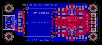
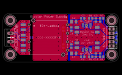
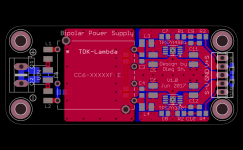
I just changed the design a bit by making the input copper pour tidier and lifting the screen copper pour to the top layer. Now the screen and the output GND connect together near the DC-DC converter common terminal.
I follow your comments but there are still some concerns which, as you mentioned, will be hard to check/prove without performing comprehensive measurements (which is not possible for me as a diyer).
I did consider using bifilar choke at the input and making the input lines fully symmetric (electrically) to balance the impedances. I dropped this idea since it would make the board much bigger than it is now due to high current capability (2~3A) chokes being really big compared to the rest of the circuit. Also, such a choke will not remove the spike noise due to high parasitic capacitance of its windings and thus I'll still need ferrite beads and capacitors as per manufacturer recommendations. All these would add to the space and the cost of the overall solution.
In principle my main concern is the emitted noise in the RF range, just to prevent it from coupling into the line level circuits within the same enclosure. Conducted noise back to the power source from the DC-DC input is less of a problem for me. I hope that my solution as it is now will help to control both radiated and conducted noise to a degree sufficient for my needs.
As for the capacitive coupling between the input and the output, the space between input and output GND planes in my design is around 1.5mm which I assume is sufficient distance to eliminate any meaningful capacitance between the two but I can easily make it bigger if necessary.
I just changed the design a bit by making the input copper pour tidier and lifting the screen copper pour to the top layer. Now the screen and the output GND connect together near the DC-DC converter common terminal.
Attachments
For the level of suppression of ringing that you are seeking you are going to need to either design your own converter, with all ringing sources damped (which usually translates into slightly lower low-load efficiency and slightly higher part count), or add a common mode choke at the input, with capacitors properly placed. Industrial is industrial, reliable, but designed to comply with EMI standards, not for unmeasurable EMI or clean good looking EMI residual waveforms.
Thanks for the comments, Eva and trobbins!
Unfortunately designing my own switcher is out of question at the moment due to lack of experience with such circuits. As for the common mode choke at the input, I've considered it at the beginning but discarded due to its size. Sufficient current rating common mode chokes are usually as big as DC-DC converter modules themselves or even bigger. In contrast, adding another ferrite bead into the opposite polarity right under the existing one seems to be easy to implement. I'll see how it will look like in the layout.
Oleg
There is no way you can reach expected result without increasing your knowledge about magnetics and switching power conversion. CM chokes for low voltage are not that big. Additionally there are ready made ICs and chokes/transformers for this application. For example most good soundcards include a DC-DC converter. Check component stores with good online catalogs such as Digikey, Mouser, Arrow, Avnet, or similar.
I agree that in order to reach good result one has to invest in learning about the subject. In my case - I do know the theory of electromagnetism and, but I lack practical knowledge in circuit design for switch mode converters. Not having the time and equipment to competently design such circuits from scratch I decided to go with the industrial grade converters as building blocks and try to attenuate their noise with external components. Whether I'll succeed in this I will only know when I try it, so stay tuned")
Thanks for your help!
Thanks for your help!
Take a look. The following link shows a selection of suitable parts.
https://www.digikey.es/products/en/...011&page=1&quantity=0&ptm=0&fid=0&pageSize=25
https://www.digikey.es/products/en/...011&page=1&quantity=0&ptm=0&fid=0&pageSize=25
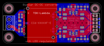
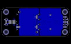
After a bit more searching I finally found smaller common mode chokes which would fit the PCB. The updated PCB design and schematic are attached.
Attachments

The schematic is not updated with CM filter.
In PCB at least one capacitor between input ground and output ground is needed to make CM filter effective. Adjust cap. value so that 1/(2*3.1415*SQRT(L_CM*C)) is well below the switching freq. of the converter.
The symmetrical layout of input inductors is not needed, one inductor in +V is enough, or even no inductors since CM mode filters have the advertised magnetizing inductance for CM filtering, plus some leakage inductance (1~10% of L_CM typ.) that does the same job as the inductors shown in PCB in +V and -V.
Thanks for the comments, trobbins and Eva!
Updated schematic is attached.
As for the symmetry and such, the PCB allows skipping optional parts should they be not needed, so I think I'll keep the symmetric layout.
According to the datasheets that I looked at the leakage inductance of the CM chokes is usually too low to do anything to the differential noise and ripple. This is one of their advertised features - undistorted differential signal. Thus the need for the differential filtering remains.
I'll seize the capacitors appropriately, but going too low in frequency will not be possible with relatively small value CM choke (due to limited physical size allowed by PCB space).
I'll experiment with the values and see where it brings me.
Regards,
Oleg
Attachments
- Status
- This old topic is closed. If you want to reopen this topic, contact a moderator using the "Report Post" button.
- Home
- Amplifiers
- Power Supplies
- DC-DC converter based PSU for line level applications