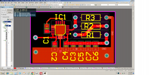
please have a look for the TPS7A4701 regulator and the through hole resistors are chosen as I have the resistors in stock as well I always like the sound of through hole resistors then SMDs.
Can anybody give me inputs about the pcb layout any improvements on this.
Can anybody give me inputs about the pcb layout any improvements on this.
Attachments
How can PTH resistors in a PSU sound different from SMD?
This would be much better on a two layer board with a ground plane underneath for both noise, heat removal and better regulation. Further the resistors are feedback so smaller less inductive SMD would be better. The ground connections to the device are too small so it may overheat in use.....
This would be much better on a two layer board with a ground plane underneath for both noise, heat removal and better regulation. Further the resistors are feedback so smaller less inductive SMD would be better. The ground connections to the device are too small so it may overheat in use.....
TI have very specific recommendations for this chip - If you want to obtain anything like its datasheet specs, layout is very important for lots of reasons, not least is planning the thermal budget correctly (hint: you have no heat sink plane).
As NO AUDIO is passing though any of these devices, use of PTH vs. SMDs will have absolutely no effect on the resulting sound - what DOES matter is the output decoupling & filtering.
Read the datasheet fully. Look at the example board that TI provide. Note the rationale for the various component & layout design decisions.
Last edited:
yes the perforated heatsink on the base of the part is left to do but.
Agreed regarding the heat Im using a external heatsink on the IC.
Does copper sucks out heat faster?the difference between the alu and copper in the amount of dissipation is very little but the faster heat sucking is copper?
Agreed regarding the heat Im using a external heatsink on the IC.
Does copper sucks out heat faster?the difference between the alu and copper in the amount of dissipation is very little but the faster heat sucking is copper?
The primary heat conduction path for the QFN (RGW) package is through the thermal pad to the PCB. The
thermal pad must be soldered to a copper pad area under the device. Thermal vias are recommended to
improve the thermal conduction to other layers of the PCB.
If you are thinking of using a heat sink on the top surface of the part, you are not going to remove the heat.... The heat is removed from the die by using the thermal pad... and by the correct use of thermal vias.
Your starters:
http://www.ti.com/lit/an/sloa122/sloa122.pdf
http://www.akrossilicon.com/home/su...racterization-and-qfn-layout-guide-rev0-6-pdf
http://cache.freescale.com/files/sensors/doc/app_note/AN4530.pdf
and IPC-7093 if you can find it.
You have already nice pcb made by Mravlcax. Works excellent. I always use 600ohm or 100-150uh ferrite bead after reg. for more smoth refined sound.
http://www.diyaudio.com/forums/vendors-bazaar/263618-tps7a4700-low-noise-ldo-regulator-pcb-8.html
http://www.diyaudio.com/forums/vendors-bazaar/263618-tps7a4700-low-noise-ldo-regulator-pcb-8.html
If you are thinking of using a heat sink on the top surface of the part, you are not going to remove the heat.... The heat is removed from the die by using the thermal pad... and by the correct use of thermal vias.
Your starters:
http://www.ti.com/lit/an/sloa122/sloa122.pdf
http://www.akrossilicon.com/home/su...racterization-and-qfn-layout-guide-rev0-6-pdf
http://cache.freescale.com/files/sensors/doc/app_note/AN4530.pdf
and IPC-7093 if you can find it.
but I see alot of designs to have heatsink on the top.
can we use a heatsink below?
but I see alot of designs to have heatsink on the top.
can we use a heatsink below?
Below, yes if you are able to mount the device upside down to reach its heath conductive bottom and be able to connect it to the heathsink. Sure.
Regards
but I see alot of designs to have heatsink on the top.
can we use a heatsink below?
Then they are wrong, I don't recall seeing any design with a heat sink on the top for these sort of devices (Plastic QFN or QFP's).
The first page of the first link shows the problem of a heat sink on the top... the heat has to go through the plastic, the thermal resistance is huge. The die is mounted upside down on the thermal pad to give the best possible thermal path for the removal of heat directly from the die.
Generally if you look at the data sheet there will be a graph of copper area the device is soldered to and the power and thermal derating etc.
hmm true...Then they are wrong, I don't recall seeing any design with a heat sink on the top for these sort of devices (Plastic QFN or QFP's).
The first page of the first link shows the problem of a heat sink on the top... the heat has to go through the plastic, the thermal resistance is huge. The die is mounted upside down on the thermal pad to give the best possible thermal path for the removal of heat directly from the die.
Generally if you look at the data sheet there will be a graph of copper area the device is soldered to and the power and thermal derating etc.
- Status
- This old topic is closed. If you want to reopen this topic, contact a moderator using the "Report Post" button.
- Home
- Amplifiers
- Power Supplies
- TPS7A4701 regulator pcb design made pls check