Howdy
I need a little low current power supply to produce +- 12V. The 5VA 2x18V transformer will be sitting on the PCB and so generally space will be very limited.
I was thinking about using either the Fairchild MDB6S or DF10S SMD bridge rectifiers rather than a bank of discrete diodes to conserve space. I am, however, a bit baffled by the thermal considerations descriptions in the dottiest with the DF10S being the most confusing.
The data sheet for the MDB6S says the device only needs 35mm^2 of board space (the device is much smaller) while the thermal characteristics are given for a "device mounted on FR-4 PCB with board size = 76.2 mm x 114.3 mm (JESD51-3 standards)."
My total board size can only be about 8x10cm, on which I need to fit the transformer, 2 rectifiers, filter caps, regs, connectors etc, and so I will need to cram things in. (It may not even be possible.)
Can anyone provide guidance regarding interpreting the data sheet thermal considerations for the rectifiers?
Regards
Steve
Perhaps the more understandable thermal spec is with 13x13 lands for each device leg. As you are using each diode in the bridge, then the total average power loss of all four die needs to be estimated, and the multi-die measurement spec used for comparison.
Staring with say 50C/W Rja, are you going to be well below the 150C Tj max at max ambient temp around the local pcb environment, and at max loading of the equipment?
You could use PSUD2 to determine rms current levels in each diode, and use forward voltage curves to estimate an average on voltage, given that instantaneous pulse power is high, but will average out in the thermal mass and thermal resistance.
Once you have an estimate for Tj max, then you can assess how your pcb compares with the 13x13 land scenario. Perhaps you are using thermal vias to move heat to the other side of the pcb, or have other ways for heat to transfer away.
Hi. I did a rough 'n ready sim in LTspice. I just used 4 1N4148 diodes to simulate the bridge (0.3A continuous current rating but built in LTspice models). The trafo I will be using has a secondary current rating of just 167mA per secondary. (Each secondary will have its own bridge.) The real load won't get close to this but for the sake of investigation I loaded the sim circuit (typical LM317 reg circuit set for 12V) with a resistive load of just under 80mA equating to just under 200mA RMS at the secondary. Power dissipation for each bridge diode is about 46mW - let's say 200mW for 4. Vf for the MDB6S is lower than for the 1N4148 and so this is even more conservative.
I think that implies being under the Tj 150C limit for even relatively high ambient temperatures. Even more so with more realistic load assumptions.
But then I found I had board space, chickened out and slotted in a bunch of 1N4007 in DO41.
I think that implies being under the Tj 150C limit for even relatively high ambient temperatures. Even more so with more realistic load assumptions.
But then I found I had board space, chickened out and slotted in a bunch of 1N4007 in DO41.
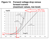
As the Tj rises the Vf falls.
So the power dissipated in the diode rises less fast than the increase in current would make you believe.
1A bridge, or 1A diodes, would do equally well for a 80mA supply.
300mA continuous is a lot more and then the diodes will be running hotter.
So the power dissipated in the diode rises less fast than the increase in current would make you believe.
1A bridge, or 1A diodes, would do equally well for a 80mA supply.
300mA continuous is a lot more and then the diodes will be running hotter.
Indeed. At 125C Vf of the MDB6S falls to about 0.8V at 0.8A and closer to 0.7V at 0.2A. (I assume forward current in these charts is RMS.)
Maybe I shouldn't chicken out. There will be fat traces connected to the pins of the MDB6S (76mil), a good sized PCB and I could always add a few vias to GND underneath the device to help with cooling also? Also, any final post reg load will be lower than 80mA (which would place a demand on the transformer secondary which exceeds its rating). Less than half that would be a better assumption.
Maybe I shouldn't chicken out. There will be fat traces connected to the pins of the MDB6S (76mil), a good sized PCB and I could always add a few vias to GND underneath the device to help with cooling also? Also, any final post reg load will be lower than 80mA (which would place a demand on the transformer secondary which exceeds its rating). Less than half that would be a better assumption.
Fairchild have a Spice model for the MDBS10SV which is in the same class of devices. It has a higher current rating and is less well optimised for Vf. I dropped this into my quick 'n dirty LM317 reg model. I then loaded the reg output to achieve approx 170mA AC current at the input to the bridge (slightly higher than the transformer secondary rating). Modelled dissipation of the MDB10SV is 96mW. Taking the dual dice junction to ambient spec of the MDB6S of 250C/W means a conservative - I think - 25C rise above ambient with nothing special done to the board. I think I will give them a go.
the current is continuous DC.Indeed. At 125C Vf of the MDB6S falls to about 0.8V at 0.8A and closer to 0.7V at 0.2A. (I assume forward current in these charts is RMS.)
Maybe I shouldn't chicken out. There will be fat traces connected to the pins of the MDB6S (76mil), a good sized PCB and I could always add a few vias to GND underneath the device to help with cooling also? Also, any final post reg load will be lower than 80mA (which would place a demand on the transformer secondary which exceeds its rating). Less than half that would be a better assumption.
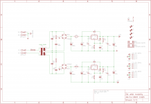
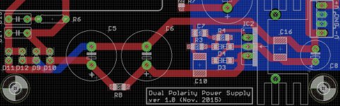
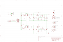
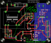
Here's what I have done at this point. What do you guys think? Good, stupid, dangerous, can be improved?
I used fat traces into / out of the two MDB6S. BR1 sits above the (masked) ground plane on the bottom of the board (blue) and I placed a few via underneath the MD6S to allow heat to flow to the bottom layer more readily. Underneath the second MDB6s I placed an unmasked solder pad, and again placed some vias underneath the MDB6S. I am getting overlap DRC errors for this latter setup but surely this is okay.
Thoughts? Any guidance welcomed!
Attachments
Last edited:
Hi Pafi. Thanks for the response.
I will move the trace going from the secondary to C11 to the right. The distance between the right fuse pad and the pads at the top of C11 and C12 is just over 200mil. Not enough? I understood the requirement is 120mil for products protected by earthing (Class I; 230V).
I was wondering about R5/R6 and R7/R8. Will change R5/R6 to SMD - 0.25W resistors ok? - and move C11, C12 and BR1 down.
What would you suggest for R7/8? In normal use (up to and beyond the rating of the transformer secondary) the dissipation is tiny but I take your point re overload although I fear the transformer would be in dire shape in such a situation.
Any views on how I have attempted to keep BR1 and BR2 cool?
Why not use a fast recovery bridge diode such as CBR1U-D020S, and hence do away with your perceived need for snubbers. You may then be able to minimise the AC secondary circuit loop area, and even avail yourself of a smt ceramic cap right on the bridge output terminal in order to bypass any perceived higher frequency noise that may exist.
Wouldn't the regulator reference connection to 0V be at the output side capacitor terminal, rather than along the trace back to the input capacitor where it will pick up load induced parasitic voltage signals.
Wouldn't the regulator reference connection to 0V be at the output side capacitor terminal, rather than along the trace back to the input capacitor where it will pick up load induced parasitic voltage signals.
I'd suggest considering 4xSTPS2L60 thru hole Schottkys mounted vertically. There's a transformer on the PCB and there's also a vertical fin heatsink, so you've got more than enough (0.6") vertical height. Mounting the diodes vertically reduces their area footprint. The diodes are "only" rated for 60V but your transformer delivers 15V RMS, and it's a bridge configuration, so the diodes won't see more than 23V of reverse bias. Round that up to 50V, you're still fine.
Because these are low voltage Schottkys, their forward voltage drop is small (0.45V at 500mA) so self-heating P=IV is reduced. And, since these are 2 amp rated diodes, but operated at 1/2 amp, you have plenty of safety margin.
Also, it might be worthwhile to measure your transformer secondary before shipping out your Gerber files for PCB manufacturing. For low-VA-rated Class B transformers, I've seen shockingly high secondary leakage inductance. So high that sqrt(L/(Ct+Cr)) is many tens of kilohms. This means you can get an optimum (zeta=1.0) snubber with a single component -- merely a ~ 22K resistor (!!) -- and it dissipates negligible amounts of power. No series Cs is needed because power is neglible. No parallel Cx is needed if you aren't a clueless newbie with no prior exposure to second order linear systems. Just a thought. It might be a cute way to remove two components from the PCB while maintaining guaranteed optimal damping.
__
Attachments
Why not use a fast recovery bridge diode such as CBR1U-D020S, and hence do away with your perceived need for snubbers. You may then be able to minimise the AC secondary circuit loop area, and even avail yourself of a smt ceramic cap right on the bridge output terminal in order to bypass any perceived higher frequency noise that may exist.
I think it is better to snub than omit it and hope the bridge diode doesn't induce ringing. But I take on board Mark's comments below regarding potential optimisation of the snubber.
Wouldn't the regulator reference connection to 0V be at the output side capacitor terminal, rather than along the trace back to the input capacitor where it will pick up load induced parasitic voltage signals.
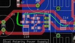
Do you mean, for example, shifting the 0V connection for C7 and R3 past the 0.1uF output bypass cap (and relocating components to minimise trace lengths)? See attached graphic. I only routed 0V for the -12V reg. For the +12V reg I only routed 0V from bridge (then an SMD component on the top layer) to the first filter cap and on to the second. Thereafter it's the bottom layer ground plane. My thinking re this was, rightly or wrongly, (a) I needed a low impedance path to 0V/GND for the bridge and routine to the filter cap seemed a lot better than a via, (b) routing to the second filter cap was easy and ensuring close tracking of flows to and from the caps, (c) to route 0V/GND beyond this point was more circuitous. Assuming the plane remains in place I would not know how to apply your comment to the +12V reg. For the -12V reg it just seemed very weird to have the LM317 output (and Vref resistor R4 etc) connected to just the bottom layer GND plane; it was also easy to continue the routing of 0V to the output cap C8 at which point it connects to the bottom layer GND plane.
I'd suggest considering 4xSTPS2L60 thru hole Schottkys mounted vertically.
Ok. (I just think SMD is sexy.
)Also, it might be worthwhile to measure your transformer secondary before shipping out your Gerber files for PCB manufacturing. For low-VA-rated Class B transformers, I've seen shockingly high secondary leakage inductance. So high that sqrt(L/(Ct+Cr)) is many tens of kilohms. This means you can get an optimum (zeta=1.0) snubber with a single component -- merely a ~ 22K resistor (!!) -- and it dissipates negligible amounts of power. No series Cs is needed because power is neglible. No parallel Cx is needed if you aren't a clueless newbie with no prior exposure to second order linear systems. Just a thought. It might be a cute way to remove two components from the PCB while maintaining guaranteed optimal damping.
__
Clueless newbie describes me well. I will have to take a look at the Quasimodo Jig design note (and previous second order system reading references) to obtain insight into why Cs and Cx isn't needed. (Perhaps this is an interesting sub topic for the Quasimodo thread...)
Regarding R7 and R8, just how conservative should one be regarding wattage rating for these? Again, in normal operation (currents up to the secondary rating of the transformer) dissipation is tiny at circa 16mW...
Attachments
(I just think SMD is sexy.
If you're really worried about thermal considerations, you could buy a few of these Aavid products or possibly those other Wakefield products. Again you'd be taking advantage of the large permissible height-above-board, thanks to the big transformer and big finned heatsink on the same PCB.
You can use a Dremel tool to cut them to a perfect size, glue them on, and reduce worry. Or maybe you would enjoy worrying about the long term reliability of the glue. You could intentionally cut it big so it sticks out beyond the package by a few mm, and then use another daub of glue to adhere to the PCB. Now you're glued three places: once to the IC and twice to the board. At the cost of some additional area. Rework? Oy vey.
To my mind, good management of rectifier induced noise includes minimising the loop area of rectification current pulses, and minimising coupling of high dV/dt circuits to the rest of the world.
SMT devices are great at minimising loop area - smt diodes and smt caps allow the loop external to the transformer secondary to be made very small, especially for smt devices placed on the rear of the pcb. An smt cap at the diode bridge can minimise the loop, rather than extending the loop out to the first leaded e-cap. Adding snubber parts may introduce a compromise.
The secondary winding and attached traces become a source of high dV/dt. The diodes are a pathway of parasitic capacitive leakage, especially schottkys, as well as oversizing pn diodes.
There will be ac current flowing between C6 and C8. The terminal of C8 may be the better target for connecting the 0V reference of the regulator, if practical.
There will be ac current flowing between C6 and C8. The terminal of C8 may be the better target for connecting the 0V reference of the regulator, if practical.
Hi
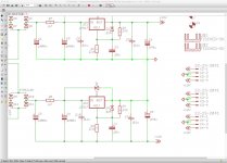
Forgive me for being a bit slow. The R4/R3 voltage divider on the -12V regulator (positive reg typology) is between 0V and -12V. The output of -12V IC2 LM317 is 0V and is connected to the 0V plane on the bottom of the board (blue). (My trace from IC2 output to C16 is necessitated as result of C16 being SMT and hence not connected to the bottom layer 0V plane. I could have used a via to the bottom layer plane and maybe that would be better. My trace from C16 to the + pin of C8 is likely highly redundant - that pin is already connected to the bottom layer 0V (blue) plane - and perhaps I should delete the trace.) So the high side of the voltage divider, 0V, is taken from IC2 output, 0V. Again, I could have used a via to the bottom layer 0V plane but given the proximity to the output pin that seemed a more appropriate place to connect 0V. The low side of R3 needs to be connected to -12V. I can connect to -12V either between C6 and C16 or between C16 and C18. I thought the former is 'normal'.
For the +12V reg, the voltage divider R2/R1 links +12V (at the output pin of +12V reg LM317 IC1) and 0V via the bottom layer 0V plane.
It seems to me the improvement I can make to address your earlier points is to ensure the 0V bottom layer plane is isolated as much as possible from the AC pulses between the bridge and the -ve pins of C1 and C2 (input filter caps C5 and C6 on the -12V side are, obviously, not connected to the plane) by routing the bridge to C1 and C2 -ve pins rather than using the 0V plane (as already done) and keeping the trace length from the secondary to the bridge to C1 as short as possible (made easier if snubber caps C11 and C12 disappear and R5 goes SMT). (Same with the second secondary through to C5.)
Make sense?
Regards
Steve
Attachments
Last edited:
Better?
- R3-C7 trace redone to just past output cap C8.
- Further optimisation can be done if snubber network simplifies to a single resistor.
- I increased R7 and R8 to 1W surface mount resistors - enough?
- I'm a bit stuck re C16. I thought I could place it on the bottom of the board but IC2 output is 0V and on the bottom plane and so I can't route a 0V/GND trace from IC2 output to C16. I guess I can place it on the top layer above D3.
- D5/D7 is routed to C1 and C2 parallel to the +ve side (rather than using the 0V plane). At C2 -ve terminal there's a connection to the 0V bottom layer plane but it has thermals and so the trace on the top layer represents the lower impedance path.
- C9 is on bottom of the board. I could do the same with C15 to get it closer to the output pin but then I start to clog up the 0V plane so probably not a good idea.
Attachments
Last edited:
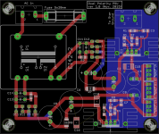
No.
The -ve of the upper bridge connects to the -ve of C1.
The -ve of the lower bridge connect to the -ve of C5.
R1 and C3 need to connect. This then connects to the output at C4.
R3 and C7 need to connect. This then connectss to the output at C8.
Once you have the schematic correct, then check to see if the PCB matches.
No.
The -ve of the upper bridge connects to the -ve of C1.
The -ve of the lower bridge connect to the -ve of C5.
R1 and C3 need to connect. This then connects to the output at C4.
R3 and C7 need to connect. This then connectss to the output at C8.
Once you have the schematic correct, then check to see if the PCB matches.
What's wrong with the circuit? All of the above are connected. I have missed a junction symbol at the low side of C7 on the circuit but that doesn't affect the circuit/board. C7 and R3 are connected as a glance at the board would show. The junction symbol is for clarity. Note the connections to GND and -12V respectively on the schematic at the relevant bridge. Also don't forget the blue traces on the bottom layer. In Eagle, where a bottom layer blue trace overlaps a top layer red trace, the combination is shown in pink. For example, D12/D9 are connected to C5 via the bottom layer. A portion of this trace is directly underneath the top layer connection from D11/D10 to C5. Hence the pink colour. Also don't forget that the blue polygon is a bottom layer 0V/GND plane.
Attachments
Last edited:
- Status
- This old topic is closed. If you want to reopen this topic, contact a moderator using the "Report Post" button.
- Home
- Amplifiers
- Power Supplies
- Thermal considerations for Fairchild SDIP bridge rectifiers