Which line exactly? -12V, +12V, GND or some other one?
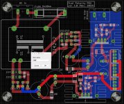
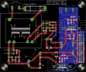
Attached images highlight traces for each of these. -12V is about as efficient as it can get given size of transformer, heatsink and output connectors. The series of traces from the +12V bridge to output are forced by virtue of the same. (As noted above, if the snubber circuits simplify to just a single resistor then there's some further optimisation available.) GND/0V has to connect in numerous places - the low side of the positive regulator, the output of the -12V LM317 and the high side of all that follows, and the connector to star ground. Routing this as a series of traces would be spaghetti. Is it not sensible to use a GND plane for this?
Attached images highlight traces for each of these. -12V is about as efficient as it can get given size of transformer, heatsink and output connectors. The series of traces from the +12V bridge to output are forced by virtue of the same. (As noted above, if the snubber circuits simplify to just a single resistor then there's some further optimisation available.) GND/0V has to connect in numerous places - the low side of the positive regulator, the output of the -12V LM317 and the high side of all that follows, and the connector to star ground. Routing this as a series of traces would be spaghetti. Is it not sensible to use a GND plane for this?
Attachments
You've lost me completely. The schematic is the same as any other I have seen using this typology including discussions on this forum in which you have participated. I realise I have omitted the protection diodes shown as D9 and D10 in Fig 11 here. This is a mistake and I will add them. I will search for potentially suitable components. Do they make the existing D1 and D3 redundant? I am missing any other issues with the schematic other than the following which could be emphasised by changes to the schematic (although the effective schematic would be unchanged).
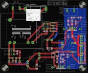
With respect to the board, I guess we can debate where to take the input to the Adj voltage dividers R2/R1 and R4/R3 respectively. Trobbins suggested moving the low side of the latter to the -ve terminal of C8 and I did this (i.e. low side of R3 senses -12V at, or rather just past, the neg reg output cap C8).
Perhaps, in like fashion, I should have R2 sense +12V at the pos reg output cap C4 or the trace to the output connectors which is closer? When I have previously looked at just single positive regulators no one (including yourself when you have assisted in these) has raised this point but if it is good practice I'm happy to run with that from now on.
In both cases the other side of the voltage divider is 0V GND. R1 connects to GND as does R4. Routing GND would be very difficult. Do you object to the use of a plane for 0V GND in this situation?
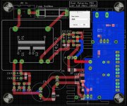
(Latest version of board attached.)
With respect to the board, I guess we can debate where to take the input to the Adj voltage dividers R2/R1 and R4/R3 respectively. Trobbins suggested moving the low side of the latter to the -ve terminal of C8 and I did this (i.e. low side of R3 senses -12V at, or rather just past, the neg reg output cap C8).
Perhaps, in like fashion, I should have R2 sense +12V at the pos reg output cap C4 or the trace to the output connectors which is closer? When I have previously looked at just single positive regulators no one (including yourself when you have assisted in these) has raised this point but if it is good practice I'm happy to run with that from now on.
In both cases the other side of the voltage divider is 0V GND. R1 connects to GND as does R4. Routing GND would be very difficult. Do you object to the use of a plane for 0V GND in this situation?
(Latest version of board attached.)
Attachments
Last edited:
Hi SGK,
Some time ago I have done similar PCB exercise as you do but never made the boards...
I am not a skilled circuit/PCB designer but what puzzles me about your design is why wouldn't you make your board symmetric? You can turn the transformer 90 degree counterclockwise and place the mains input on the left side of the board. This would nicely separate the high voltage (left) side from the low voltage (right) side. It would also give you enough space above and below the transformer to place pos/neg snubbers/bridges/CRC filters. The actual regs can then have all the space on the right side making a nice symmetric layout if you turn the regs face-to-face and place the heat sinks along the edges of the PCB for better cooling. Outputs can go in the middle of the right side of the board and if you make more GND output pins you can also have your "Star ground" (I guess it should be safety earth connection?) from there too. I also have an impression that this board is asking for through hole components. I like the SMD staff myself, but this design seems to have no benefit from it. If you still want to use SMD parts I would advise not to use the pads with "W" designation (for wave soldering). Also CRC filters can actually be CRLC if you use inductors with the appropriate DCR. It takes more or less same space.
Just my 2 ct.
Regards,
Oleg
Hi Oleg. I agree a more symmetrical typology with an LM317/LM337 pair would be easier to lay out, but I understand it better to avoid the LM337 as it has less performance than its LM317 sibling. Hence using the dual positive regulator typology to generate +/-12V. Note the different pin layouts of the LM337 versus LM317 make placing the two back-to-back easier. Two LM317 back to back means you have to resort more to the bottom layer for routing main in/out traces.
So 'symmetry' in this case would be an identical layout of +ve and -ve reg 'rails' (rather than one being a reflection of the other) - if that makes sense.
I'm constrained to an up to 8x10cm maximum as a result of using the Freeware version of Cadsoft Eagle. If you rotate the transformer, place the 230V AC input and fuse on the left side and shunt it all across so as to have >6-7mm between AC pads and the edge of the board then you are already 5cm+ into the board (i.e. over halfway) with the secondaries on the inner edge. The transformer's widest edge is also then across the narrowest width of the board. This way I can keep the secondary to bridge traces shorter.
Now maybe I should make things more symmetrical from top to bottom (as presented in the images above) but it likely yields little difference in the end. Lots of different ways to skin a cat... For now I am still trying to decipher AndrewT and I also need to order the transformer and test whether I can remove all the snubber caps. Maybe that opens up more opportunities for symmetry.
Why not use longer (wave soldering) pads? They make hand soldering much easier as does slightly extending pads for 1206 resistors.
I have same restrictions to yours (free Eagle CAD). There is one trick to it - the restriction is on the placement marks of components (their centers). Board outline can extend beyond 100x80 mm, components can do it too as long as their centers are within the 100x80 mm bounds. Also 100x80 bounds are measured from the "0" reference cross symbol.
As for the symmetry I guess it makes little difference if you use complementary LM317/337 or dual LM317 with dual secondary transformer.
The "W" SMD pads are narrower than the parts you solder but it will of course work. It just looks a bit mixed in your design since some parts have normal pads and some have narrow pads.
Regards,
Oleg
Thanks for the tip.
Re pads, fair point although one never notices once the part is soldered. I started off very conservative re SMD soldering with enlarged pads and more component spacing. I'm slowly reducing the former to recommended and packing things in closer, as well as going to smaller components themselves in some cases.
Re pads, fair point although one never notices once the part is soldered. I started off very conservative re SMD soldering with enlarged pads and more component spacing. I'm slowly reducing the former to recommended and packing things in closer, as well as going to smaller components themselves in some cases.
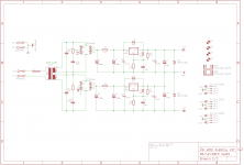
I realise I have omitted the protection diodes shown as D9 and D10 in Fig 11 here. This is a mistake and I will add them. I will search for potentially suitable components. Do they make the existing D1 and D3 redundant?
I'm wondering if Panasonic DB2441700L (data sheet) would be a suitable choice. Rated for 5A and 40V and conveniently small. The LM317T-DG (data sheet) limits at a maximum of 2.2A. Mark has previously provided guidance for such protection diodes here.
I suggest that those diodes should be rated for a current at least equal to the larger of (i) (Vprimary/Vsecondary)*Primary_fuse_current ; (ii) the current rating of the downstream fuses in the DC rails ; (iii) the output current limit value of the voltage regulators
Perhaps, in like fashion, I should have R2 sense +12V at the pos reg output cap C4 or the trace to the output connectors which is closer?
I have made this change but have stuck with the 0V GND plane for now...
SGK, I can't see any problem with your schematic or layout. I can only think that Andrew is trying to push for a schematic that shows how the node busses are more illustrative of how the pcb layout is done - but schematics are always going to fail on that aspect (which is what catches out many people starting on their first layout from just a schematic).
As you are only using a standard regulator, and not some special ultra low noise model, then most tweaks now are going to be unmeasurable - and are more up to you to balance their practicality.
As you are only using a standard regulator, and not some special ultra low noise model, then most tweaks now are going to be unmeasurable - and are more up to you to balance their practicality.
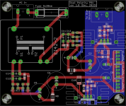
Thanks trobbins. Images of current versions are attached. I will report back when I have received the transformers and have had the chance to connect them to my Quasimodo jig.
In the interim I will work on the balanced line input board (balanced to single-ended conversion) which is one of the things that will be powered by this supply.
In the interim I will work on the balanced line input board (balanced to single-ended conversion) which is one of the things that will be powered by this supply.
Attachments
I guess the length of power traces from the filter cap to the reg is not so critical, at least datasheet does not specify max distance as far as I remember. It only recommends 0.1 uF bypass close to the reg. But may be someone more experienced could recommend the right solution.
Post31Thanks trobbins. Images of current versions are attached. I will report back when I have received the transformers and have had the chance to connect them to my Quasimodo jig.
In the interim I will work on the balanced line input board (balanced to single-ended conversion) which is one of the things that will be powered by this supply.
No !
the rectifier has TWO outputs. Those two outputs are a close coupled PAIR of wires/traces.
These MUST connect to the INPUT of the smoothing capacitors. DO NOT separate these two wires/traces to take ONE on a big separate journey around the PCB/Amplifier. That creates LOOP AREA and that creates INTERFERENCE !
The wire from the -ve sides of D5 & D7 must follow the wire from the +ve sides of D6 & D8 to feed to two terminals of C1. This is a TWO wire charging circuit. The charging PULSES must not be imposed on any other circuit.
Get the sch right first. Then design the layout to match the corrected sch.
I can only think that Andrew is trying to push for a schematic that shows how the node busses are
Last edited:
The wire from the -ve sides of D5 & D7 must follow the wire from the +ve sides of D6 & D8 to feed to two terminals of C1. This is a TWO wire charging circuit. The charging PULSES must not be imposed on any other circuit.
It does. And the pair go on to C2. By necessity, the trace from D5/D7 to -ve terminal of C1 is on the bottom layer (because it must cross the trace from D8/D6 to C1).Intentionally it is kept very separate from the GND plane all the way to C2 so that the pulses circulate locally. Exact same thing with the other regulator and C5/C6.
Last edited:
The sch shows GND at the rectifier and at the Output end of Zero Volts.It does. .............
The sch also shows -12v at the rectifier and at the Output end of -ve supply !
It does NOT .
Correct. The +ve reg rail has its bridge connected to input of IC1 LM317 (via the input filter C1/R7/C2) and GND/0V. The -ve reg rail has its bridge connected to input to the input of the second LM317 (IC2) and what becomes -12V. The schematic is in accordance with the typology shown here
Voltage And Current Regulators
Two positive regulator circuits with the 'output' of one tied to GND/0V of the other to produce -V. If it helps I can rearrange the diodes to make them look more similar but I assure you the connections are exactly the same.
So the schematic shows +12V from IC1, GND at the 'low side' of the +ve reg rail and what would normally be the output of the neg reg rail, and -12V at the 'low side' of the second reg rail.
The output connectors obviously have connections for +12V, -12V and 0V.
I can only think that Andrew is objecting to my 'shortcut' in the schematic - highlighted in the attached. Rather than showing a direct connection to C1 from the bridge I showed a connection to GND/0V. This might convey a degree of routing flexibility to a reader which, of course, one shouldn't deploy. A glance at the board would show the direct connection from bridge to filter caps has been routed properly. The reason why I have been reluctant (lazy?) to redraw the schematic is because in order to make it neat (reconfigured) I have to delete connections on the schematic and redraw them, forcing me to reroute the board - even though the traces would be identical in the end.
Edit: I am having trouble uploading the image now. I will try again later.
Edit: I am having trouble uploading the image now. I will try again later.
Last edited:
- Status
- This old topic is closed. If you want to reopen this topic, contact a moderator using the "Report Post" button.
- Home
- Amplifiers
- Power Supplies
- Thermal considerations for Fairchild SDIP bridge rectifiers