This is a technique for reducing ripple voltage on the main filtered B+ rail in a valve amp, achieved by sinking an additional dynamic current in to the B+ supply so that the B+ voltage is constant. It may be of interest to others, and can be modified to suit different aims.
The technique was inspired by restoring old valve amps that use rectifier diodes with very low peak current ratings, thereby limiting filter capacitance to often just 4-20uF. The resulting B+ ripple voltage is relatively high, and often the main contributor to hum in an unmodified amp. I have a vague recollection of seeing the technique used long ago.
B+ ripple can be lowered by a variety of modifications, such as using a different diode type, increasing first filter cap size, and adding extra RC or LC filtering stages. But the ripple filler is appealing as it can utilize the omnipresent 5V rectifier heater winding to generate a compensation voltage supply (Vcomp) of circa 10-35VDC that rides on top of the first filter capacitor voltage (Vht). A power fet then dynamically passes current from Vht + Vcomp to the output B+ supply, so as to maintain a constant B+ voltage where ripple is greatly attenuated.
The ripple filler technique allows a long conduction duty cycle of the rectifier diodes to achieve a low crest factor diode current waveform that alleviates high order mains harmonics on Vht, alleviates any contribution to mains voltage distortion, and improves the utilisation of the transformer.
However, the technique uses circuitry sitting at a high DC voltage, and is at a development stage requiring competence in many design aspects and customised application – so is not yet recommended for general diy.
My original intent was to aim for negligible ripple and hum in a guitar PP amp operating in idle, but with B+ ripple returning to near full level when the output stage is overdriven so as to retain the mains ripple character of the amp - ‘work in progress’.
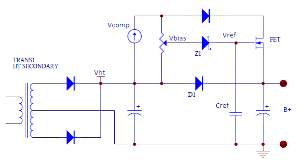
Referring to the simplified schematic, the combined voltage of Vht + Vcomp is used to charge the output B+ capacitance and maintain the load current. The FET dynamically regulates the B+ voltage to the peak of the Vht waveform, plus a small bias voltage to overcome the FET Vgs required for FET conduction. During steady-state operation, the series diode D1 stops the Vht capacitance from directly charging the output B+ capacitance, as B+ is normally higher in voltage than Vht. The reference capacitor Cref is charged by the zener diode Z1 to the max peak of Vht, plus some additional bias, and is only discharged when the min peak of Vht reduces to a level lower than Vref minus the zener voltage.
To fill the Vht ripple troughs, Vcomp and the Z1 voltage need to be at least the peak-to-peak ripple voltage. Vbias is about 4V for a typical power FET plus Z1 diode drop. The FET only needs to work at the Vcomp voltage, as protection diodes avoid any higher voltage stress. The FET current is negligible for a modern power device, so as small a device as practical is preferred to limit junction capacitances.
The intent was not to use a large capacitance on the B+ output, as it is not needed, and in general it is easier to just use a poly cap for Vht and B+ filtering (I like the 375VAC rated poly caps with DC ratings of 600V or more).
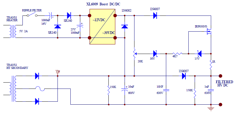
The example circuit below is my only prototype so far, and suits an amp with up to about 35Vpp ripple (ie. about 9Vrms). The Vcomp supply uses a capacitor input doubler, as that provides a common terminal for Vht and Vcomp. For the 5V heater, the doubler output needs further boosting using a XL6009 module – the module output is regulated, and can accommodate a wide input range from the doubler. The 15V zener for FET gate protection also acts to discharge Cref after turn-off. Some series resistance with the FET source can provide current limiting if needed, although that will add some residual ripple voltage depending on output capacitance.
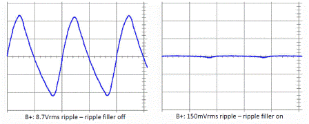
When the ripple filler circuit is on, the DC level of B+ will increase by about Vpk(ripple). With a suitable load, the example supply had 8.2Vrms original ripple which reduced to 150mVrms with the ripple filler circuit active, in which case the B+ level increased by about 12VDC. The ripple voltage waveform on Vht is close to a sawtooth, so the pk-pk voltage is about 2x sqrt(3) x the rms level. The Vht rms ripple level also increases a bit when the ripple filler circuit is active due to the constant power output characteristic of B+. Note that the ripple filler does not regulate the output voltage, and the intent was to allow natural sag to occur.
The prototype was just in a HV power supply with ss diodes, so the next step is to retrofit to an old amp and start playing around a bit more.
Ciao, Tim
PS. the doubler needed 2,000uF caps in the prototype to start the dc/dc up.
The technique was inspired by restoring old valve amps that use rectifier diodes with very low peak current ratings, thereby limiting filter capacitance to often just 4-20uF. The resulting B+ ripple voltage is relatively high, and often the main contributor to hum in an unmodified amp. I have a vague recollection of seeing the technique used long ago.
B+ ripple can be lowered by a variety of modifications, such as using a different diode type, increasing first filter cap size, and adding extra RC or LC filtering stages. But the ripple filler is appealing as it can utilize the omnipresent 5V rectifier heater winding to generate a compensation voltage supply (Vcomp) of circa 10-35VDC that rides on top of the first filter capacitor voltage (Vht). A power fet then dynamically passes current from Vht + Vcomp to the output B+ supply, so as to maintain a constant B+ voltage where ripple is greatly attenuated.
The ripple filler technique allows a long conduction duty cycle of the rectifier diodes to achieve a low crest factor diode current waveform that alleviates high order mains harmonics on Vht, alleviates any contribution to mains voltage distortion, and improves the utilisation of the transformer.
However, the technique uses circuitry sitting at a high DC voltage, and is at a development stage requiring competence in many design aspects and customised application – so is not yet recommended for general diy.
My original intent was to aim for negligible ripple and hum in a guitar PP amp operating in idle, but with B+ ripple returning to near full level when the output stage is overdriven so as to retain the mains ripple character of the amp - ‘work in progress’.
Referring to the simplified schematic, the combined voltage of Vht + Vcomp is used to charge the output B+ capacitance and maintain the load current. The FET dynamically regulates the B+ voltage to the peak of the Vht waveform, plus a small bias voltage to overcome the FET Vgs required for FET conduction. During steady-state operation, the series diode D1 stops the Vht capacitance from directly charging the output B+ capacitance, as B+ is normally higher in voltage than Vht. The reference capacitor Cref is charged by the zener diode Z1 to the max peak of Vht, plus some additional bias, and is only discharged when the min peak of Vht reduces to a level lower than Vref minus the zener voltage.
To fill the Vht ripple troughs, Vcomp and the Z1 voltage need to be at least the peak-to-peak ripple voltage. Vbias is about 4V for a typical power FET plus Z1 diode drop. The FET only needs to work at the Vcomp voltage, as protection diodes avoid any higher voltage stress. The FET current is negligible for a modern power device, so as small a device as practical is preferred to limit junction capacitances.
The intent was not to use a large capacitance on the B+ output, as it is not needed, and in general it is easier to just use a poly cap for Vht and B+ filtering (I like the 375VAC rated poly caps with DC ratings of 600V or more).
The example circuit below is my only prototype so far, and suits an amp with up to about 35Vpp ripple (ie. about 9Vrms). The Vcomp supply uses a capacitor input doubler, as that provides a common terminal for Vht and Vcomp. For the 5V heater, the doubler output needs further boosting using a XL6009 module – the module output is regulated, and can accommodate a wide input range from the doubler. The 15V zener for FET gate protection also acts to discharge Cref after turn-off. Some series resistance with the FET source can provide current limiting if needed, although that will add some residual ripple voltage depending on output capacitance.
When the ripple filler circuit is on, the DC level of B+ will increase by about Vpk(ripple). With a suitable load, the example supply had 8.2Vrms original ripple which reduced to 150mVrms with the ripple filler circuit active, in which case the B+ level increased by about 12VDC. The ripple voltage waveform on Vht is close to a sawtooth, so the pk-pk voltage is about 2x sqrt(3) x the rms level. The Vht rms ripple level also increases a bit when the ripple filler circuit is active due to the constant power output characteristic of B+. Note that the ripple filler does not regulate the output voltage, and the intent was to allow natural sag to occur.
The prototype was just in a HV power supply with ss diodes, so the next step is to retrofit to an old amp and start playing around a bit more.
Ciao, Tim
PS. the doubler needed 2,000uF caps in the prototype to start the dc/dc up.
Last edited:
Just quickly looking at JLH, it seems to use a controllable shunt current path controlled by an AC signal on the DC rail - an active load. That particular project was for lowish DC voltage rails, as all parts hang off it.
There are definite similarities with a capacitance multiplier - its unregulated, and the pass device dynamically regulates a ripple input voltage to a voltage just outside the pk-pk ripple waveform. The ripple filler increases the output voltage to above the ripple waveform, whereas the cap multiplier decreases the output voltage to below the ripple waveform.
A difference is the pass device is isolated from seeing the full input or output voltage, and so can have a relatively low voltage rating compared to B+.
Another difference is the reference signal is acquired somewhat differently - its not an RC filtered signal with RC time constant, but more like a sample and hold, and so there isn't any inherent 'capacitance multiplying' character - the output ripple is determined more by FET transconductance.
I think the protection aspects will be more robust, as shorted output is passed through a power diode.
Last edited:
I was hoping to hear a Designer's opinion on the ripple improvement capabilities of the different topologies.
Thanks for the reliability walk through. Not something I had thought of.
Thanks for the reliability walk through. Not something I had thought of.
I don't wear a hi-fi hat, so have no heavy interest in whether one or other technique is innately able to reach a lower ripple level than another. All those techniques will attenuate ripple markedly - so they all 'do the job' as I see it. So for me, the interest is pretty much in protection and in applicability.
Application is interesting as I have a guitar hat on, so PP output stage load changes and power supply dynamic response characteristics are important. Capacitor multipliers are not common in guitar amps. And strangely I went down this road as a means just to lower ripple during amplifier idle conditions, as I'd prefer a design that allows ripple to return to large levels when the amp is being pushed (not the normal aim for hi-fi).
Application is interesting as I have a guitar hat on, so PP output stage load changes and power supply dynamic response characteristics are important. Capacitor multipliers are not common in guitar amps. And strangely I went down this road as a means just to lower ripple during amplifier idle conditions, as I'd prefer a design that allows ripple to return to large levels when the amp is being pushed (not the normal aim for hi-fi).
- Status
- Not open for further replies.