I don't understand the change in output voltage at 3seconds.
That looks like your simulation has been asked the wrong question and as a result gives a daft answer.
Neither do I and, yes, I think there is a problem with the sim and TI's model for the LME49600 in particular. Hence me wanting to check the wiring of the actual circuit. My LTspice skills aren't good enough to look at the LME49600 model and identify/correct the problem.
Thanks Pafi.
Unfortunately that is unavoidable given I am using two existing (+reg) boards. The output connectors on each board can't be changed.
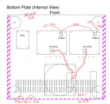
Here's my current draft layout within the enclosure. I could try rotating the PSU boards CCW 90 degrees. I was trying to keep all AC elements to the rear of the enclosure. With the rotation there would still be a GND connection wire between the boards but it would be shorter.
(The first pic in post 727 shows what an assembled reg board looks like.)
Attachments
Last edited:
I think there is a problem with the sim and TI's model for the LME49600 in particular
Maybe, but I suspect the problem is more probably in the connections or simulation parameters or auxilary parts.
What does your intuition say to you about these ideas?
Or to send (VCC,VEE) as a tightly twisted pair, with gnd tied and lashed alongside but not twisted?
- Connecting the two Vreg board "ground" connectors with very thick (10 gauge?) conductors
- Using the center point of the thick conductor as the launching point for sending "ground" from the regulation hemisphere, to the amplifier hemisphere
- Sending (VCC,ground) as a tightly twisted pair, and also sending (VEE,ground) as another tightly twisted pair?
Or to send (VCC,VEE) as a tightly twisted pair, with gnd tied and lashed alongside but not twisted?
Attachments
I understand the principle of twisting together 'flow' and 'return'. Ideally I would have a single GND point closely located to both Vcc and Vee connectors and I would twist the lot together or rather use some of my leftover Kimble Kable KWIK-16 utilising 3 of the 4 conductors. Each conductor is 16AWG.
I like the idea of bringing a length of this KWIK-16 cable to the mid point of the GND connection, attaching the conductor for the GND delivery there and twisting the (longer) conductors for Vcc and Vee, respectively, down each side of the GND connection. It's impossible to have Vcc and Vee (the flow and return for most of the current) twisted together for these last lengths but I guess this is the best that can be done.
What I did not like was the idea of using 4 conductors and only connecting the two GND wires at the amp module.
Rotating the reg boards would shorten the GND connection from 11cm to 9cm. That seems neither here nor there to me. It would mean longer AC carrying wires which I would have thought undesirable.
Last edited:
I have modeled four different op amps: TL071, LT1677, LTC1150 and AD797. I also went through a number of Mosfets for the pass transistor.
Be careful with the LT1677, it has little phase margin (30 or so), and in most regulator circuits (where it controls the pass transistor) it will ring at stepping the load. Also will start to oscillate from all kind of smallish parasitic load capacities. If you want a "text book" response at step load (w no overshoot), look at LT1001. If you want a little faster response (with slight overshoot but no ringing), and more current available to drive the transistor, then LT1881 and LT1884 are worth investigating.
Also if you get bored with the MOSFET pass transistor and want a nice easy to drive bipolar, check 2SC6144SG (available chez Digikey).
")
Be careful with the LT1677, it has little phase margin (30 or so)
The LT1677's phase margin is very, very good (> 60 degrees) unless you do something very silly: operate it with a common mode input voltage less than a volt from the bottom supply rail. I've attached a datasheet figure showing phase margin when the common mode input voltage is halfway between the rails.
In the SuperRegulator circuit design, the expected operating point for the opamp inputs is about halfway between the supply pins, with the types of VREF sources (bandgap shunt ICs, buried Zener ICs, etc) people are likely to use when making a voltage regulator.
Attachments
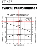
The LT1677's phase margin is very, very good (> 60 degrees) unless you do something very silly: operate it with a common mode input voltage less than a volt from the bottom supply rail. I've attached a datasheet figure showing phase margin when the common mode input voltage is halfway between the rails.
In the SuperRegulator circuit design, the expected operating point for the opamp inputs is about halfway between the supply pins, with the types of VREF sources (bandgap shunt ICs, buried Zener ICs, etc) people are likely to use when making a voltage regulator.
There's a problem with either the datasheet or the spice model supplied with LTspice. Try the attached ltspice schematic , the transistor model is available from ON Semi (or you can use any medium/high power transistor with decent fT and hfe). Diodes you can replace with any generic rectifiers >= 1A. Look at the transient response. Then replace LT1677 with LT1881, LT1884 and LT1001 for a change. Interesting?
Attachments
Last edited:
I also found Figure 4 in the document here:
https://www.maximintegrated.com/en/app-notes/index.mvp/id/3443
to be useful in trying to estimate the phase margin of the whole circuit, just by looking at the step response.
https://www.maximintegrated.com/en/app-notes/index.mvp/id/3443
to be useful in trying to estimate the phase margin of the whole circuit, just by looking at the step response.
Good. I recommend you assign "trustworthiness=0.80" to whichever member of the set {simulation, datasheet} best matches your own measured data on real circuits using real test equipment. I recommend you assign "trustworthiness=0.20" to the other member of the set {simulation, datasheet} which is the second best match.
Good. I recommend you assign "trustworthiness=0.80" to whichever member of the set {simulation, datasheet} best matches your own measured data on real circuits using real test equipment. I recommend you assign "trustworthiness=0.20" to the other member of the set {simulation, datasheet} which is the second best match.
Alternatively both information sources are correct but incomplete in different ways.... As you may notice from the datasheet, they only characterize the phase margin vs frequency at CLoad=10pF. And temperature characteristics at CLoad=15pF. Those graphs showing gain/phase vs a set of CLoads in current sinking/sourcing situations are conspicuously missing.
For hilarity you can replace the pass transistor with one with known high Cibo (or add some small parasitic caps in the schematic). You'll see very long ringing trails or outright oscillations.
I'm still slowly progressing through this epic thread... so please bear with me with a few more questions.
As theory predicts and the practical transient response measuring difficulties mentioned in this thread have confirmed, the benefits of using fast op amps are diminishing with the length of wires between the regulating device and the load. The longer the wires, the more it looks like a "driving cables" problem - where, as we know, it's more about matching impedances than having stiff sources with low Z and fast response.
Surely we could "improve" the supply by using an AD8045 and a matched RF transistor? Or maybe not? How can we decide that the op amp speed is "good enough" for the concrete situation we're in?
(of course I do understand that as DIYers we also do lots of things "just because we can" lol but seeing for example Jung supplies connected with 2 feet long wires to the load still raises some questions )
As theory predicts and the practical transient response measuring difficulties mentioned in this thread have confirmed, the benefits of using fast op amps are diminishing with the length of wires between the regulating device and the load. The longer the wires, the more it looks like a "driving cables" problem - where, as we know, it's more about matching impedances than having stiff sources with low Z and fast response.
Surely we could "improve" the supply by using an AD8045 and a matched RF transistor? Or maybe not? How can we decide that the op amp speed is "good enough" for the concrete situation we're in?
(of course I do understand that as DIYers we also do lots of things "just because we can" lol but seeing for example Jung supplies connected with 2 feet long wires to the load still raises some questions
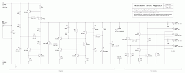
)No, the biggest improvement available in a redesign-everything-from-scratch, full do-over, would be to integrate the test circuits INTO the psu circuit board. Another DIYA member has done so, in a sub-100-milliamp power supply, HERE (schematic copied below). Notice that the designer has placed the power dissipation resistors in the source leg, not the drain leg, of the testing MOSFET. This allows both sinewave and squarewave (and in fact any arbitrary waveform) test currents to be applied. A total PSU redesign might include this type of test circuitry AND the squarewave-only test circuitry with resistors in the drain leg.
Also notice the explicit connectors for low-parasitics attachment to oscilloscopes.
Also notice the explicit connectors for low-parasitics attachment to oscilloscopes.
Attachments
But isn't this an exercise in "improving" just the PSU itself in some abstract test measurements, with little consideration to what it will be actually driving in real world?
If your project is let's say powering a VC-OCXO with minimal induced phase distortion, then in the final version of the board you have the privilege of being able to place the OCXO right next to the regulating device(s) - so the test board above would make perfect sense in trying to optimize the PSU.
However, when the load consists in separate boards connected with wires, shouldn't we also give more attention to how the PSU will behave with that particular load?
- Status
- This old topic is closed. If you want to reopen this topic, contact a moderator using the "Report Post" button.
- Home
- Amplifiers
- Power Supplies
- Adventures with 5A regulated voltage circuits