Ok I was no thinking bidirectionally (obviously). Thanks.
I will try to work on this some more tonight, including taking Jan's advice re Q3. The zener clamp will likely have to wait for parts (unless I wanted to rig it with LM329s or attempt to use SMD parts).
The zener clamp will have to wait until you get it to work first ;-)Just hang a zener that you have around between S and G. Anything from 5V to 15V will be OK
; ok
I didn't get any time on this this evening except to remove the MOSFET. My multimeter is showing continuity between all three pins so it's toast.
I also realise I missed one observation in my measurements in post #437 - the op amp output is 5V below that of the gate. So at least Z3 is now working with the part placed correctly for its pin configuration. And, yes, I do realise each set of measurements has yielded different values as various things have not been working. So ignore each set of previous measurements.
When I have replaced the MOSFET, removed Q3 and dropped in the 1K resistor I will post a new set of results.
Thanks for sticking with me on this.
The point is that you need enormous amount of energy to have "fast regulation" with such large capacitive load and you don't have it in you circuit.
Output capacitor will define your regulator speed, larger capacitor means slower regulatin and vice versa.
It is pointles to have ultra high speed driver and NFB when those output capacitor will "ruin" all that.
Take an look on original Jan's schematic, how much capacity they put at regulator's output. You put almost 20x higher capacity ...
Last edited:
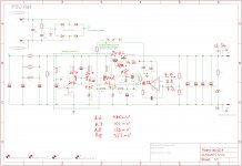
Some progress. I replaced the pass MOSFET, removed Q3 and soldered a 1k resistor over Q3's emitter and collector pads.
Attached is the circuit with voltage readings added. I used my cheap multimeter rather than scope. Note it may be reading a little high as previously I had measured the voltage at the LM329 Z2 and observed 6.95 whereas the multimeter is reading 7.13.
At least I am back to having circa 12V out now. The current source/mirror still doesn't appear to be working to a tolerance I would expect and Z1 is reading lower than expected.
Attachments
and you don't have it in you circuit.
Explain
Explain
http://www.ti.com/lit/wp/snoa842/snoa842.pdf
Some 99 percent of the "design" problems associated with linear and switching regulators can be traced directly to the improper use of capacitors: wrong type, wrong value, or incorrect physical placement.
Last edited:
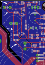
Hmmm, a review of the layout shows that the VIN wire which supplies all three branches of the current source, is in fact a relatively narrow trace (a/k/a copper resistor) with 40-80 squares of resistance (thus 20-40 milliohms). See white arrows in attached image.The current source/mirror still doesn't appear to be working to a tolerance I would expect ...
The voltage drop along this resistor is pretty small, and does not account for all of the mismatch. If there's 5mA per leg, plus 10mA for the opamp leg (R6) that means the upstream piece of the 1:1:1 mirror {namely R9+Q3} has a half millivolt to a full millivolt more supply.
But still I'd widen it on the next revision.
Attachments
Yu3ma, thanks for the link. At a glance it covers material I have read before. You claimed the output caps weren't in my model. They are, as are assumptions (and sensitivities) regarding their ESL and ESR. Take a read from about post #235 to #271 within which we discussed output caps, their ESR and ESL and the impact on modelled output impedance, transient response and stability margins.
But still I'd widen it on the next revision.
With Q3 lifted there's just the Q1/J1 current source and its mirror Q2 - resistors R7 and R8 are much closer to each other than is R9.
The trace is 24mil in 2oz. I'm rather hoping not to have to do the boards again but will make the amendment if I do.
") I would also wonder if there are benefits to using a single IC with multiple PNP transistors in the one package...
I would also wonder if there are benefits to using a single IC with multiple PNP transistors in the one package...When I laid out the board, I was hesitant with regards to the routing of J1's gate and source to each of the bases of the PNP transistors, C7 and the collector of Q1. Anything wrong there or something might be improved?
Last edited:
Some progress. I replaced the pass MOSFET, removed Q3 and soldered a 1k resistor over Q3's emitter and collector pads.
Attached is the circuit with voltage readings added. I used my cheap multimeter rather than scope. Note it may be reading a little high as previously I had measured the voltage at the LM329 Z2 and observed 6.95 whereas the multimeter is reading 7.13.
At least I am back to having circa 12V out now. The current source/mirror still doesn't appear to be working to a tolerance I would expect and Z1 is reading lower than expected.
Well the reg seems to work fine now, well done!
(Aside note: why no supply the opamp and the ref from Vout instead of Vin? Much cleaner supply.).
Anyway, lets now tackle the other stuff.
[And don't get distracted by the output cap - the only negative effect would be too high transient trough the *** FET at switch-on, so for the next tests you may want to lower it to just one of the caps shown.]
TBH can't see anything wrong with the current mirror stuff. The idea is that Q3 carries the same current as Q1, right?
Now that it all works, why not try to insert Q3 instead of the 1k and see what happens? But do lower the output cap value to save the FET.
Jan
Last edited:
The point is that you need enormous amount of energy to have "fast regulation" with such large capacitive load and you don't have it in you circuit.
Not really. You can reason that because the cap is so large it can only change in voltage very slowly so the reg can easily keep up with that.
I do agree that it is rather high but more from the point of inrush current limiting at switch-on - ultimately that may be what killed the FET.
OTOH, that cap really is only there for stability and 50uF would probably work just as well (and be cheaper and smaller).
Jan
(Aside note: why no supply the opamp and the ref from Vout instead of Vin? Much cleaner supply.).
Thx.
Errr.. his memory is straining to work. I think we discussed this one at some point in relation to the Jung/Didden super reg. And I recall the issue is more difficult when the pass device is a MOSFET. I think when I started looking at MOSFET series pass regs I didn't have the level shift in which case there's nothing to get the gate going if the op amp is driven from Vout (whereas the Jung/Didden reg has to bias the pass device from Vin). Of course the 5V and 3V3 versions won't have level shifts but the 12V reg will supply power to their op amps and Vrefs.
Not really. You can reason that because the cap is so large it can only change in voltage very slowly so the reg can easily keep up with that.
Yes, and it aided output impedance and transient response. Of course, one doesn't want phase and gain margin/stability impairment. Phase margin is better with the larger capacitance.
As regards in-rush, I guess that's a valid concern. The IPP037N06L3G is rated for 90A continuous drain current, but of course when Vds is large - at startup - the safe operating level of Id is much lower. That said, the power rail had been cycled into operation many times before the FET blew and ahead of the power rail is in-rush limiter. I will take a closer look at what my model suggests the Id versus Vds of the pass transistor is.
Removing caps is easy however...
I am still bugged as to why a 2% voltage tolerance 10V zener (which had measured such previously) is reading closer to 9V...
Last edited:
- Status
- This old topic is closed. If you want to reopen this topic, contact a moderator using the "Report Post" button.
- Home
- Amplifiers
- Power Supplies
- Adventures with 5A regulated voltage circuits