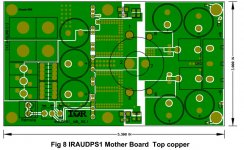
This is a top layer of an audio amp by IR in their AP note "iraudps1.pdf".
The layout looks like it was carved out of a solid copper layer, almost as if there was an anti trace command that lays down voids in the copper instead of traces.
I never heard of an anti trace command so it was probably copper fills. But even so it really looks like it was carved out, not poured.
Does anyone know what the procedure is for laying out a board like this.
Attachments
The layout looks like it was carved out of a solid copper layer, almost as if there was an anti trace command that lays down voids in the copper instead of traces.I never heard of an anti trace command so it was probably copper fills. But even so it really looks like it was carved out, not poured.
Does anyone know what the procedure is for laying out a board like this.
This particular pcb was made in the usual way, with a layout program that can "copper pour" in the blank areas,
with a small space left between the pour areas, and the traces and pads. Many recent programs can do this.
There are also pcb engraving machines that can make a single pcb that looks similar, but these pcbs lack plated through holes,
solder mask, and silk screen.
Last edited:
This particular pcb was made in the usual way, with a layout program that can "copper pour" in the blank areas,
with a small space left between the pour areas, and the traces and pads. Many recent programs can do this.
There are also pcb engraving machines that can make a single pcb that looks similar, but these pcbs lack plated through holes,
solder mask, and silk screen.
So did they first draw out all of the shapes of the pours and then use a fill command?
And how are the traces handled. If you have a large copper pour area and it has traces in it, does the defined area just fill up with copper and flow around pre-existing traces with a specified clearance?
So did they first draw out all of the shapes of the pours and then use a fill command?
And how are the traces handled. If you have a large copper pour area and it has traces in it, does the defined area just fill up with copper and flow around pre-existing traces with a specified clearance?
Normally the blank areas are automatically filled with the command, using a specified clearance from the pre-existing traces, pads, etc.
You don't have to draw the shapes, the pour is just set back from the existing copper areas.
Eagle does this, and there's a free version. http://www.cadsoftusa.com/download-eagle/freeware/?language=en
Last edited:
Normally the blank areas are automatically filled with the command, using a specified clearance from the pre-existing traces, pads, etc.
You don't have to draw the shapes, the pour is just set back from the existing copper areas.
Eagle does this, and there's a free version. Free EAGLE PCB Design Software, Layout Software - CadSoft Freeware
I can understand a basic copper fill were it flows around all other copper and the fill is just a poor mans ground plane. But in this case the copper fill is actually the routing of the circuit. That is what i am impressed with. Very high current low impedance traces.
I can understand a basic copper fill were it flows around all other copper and the fill is just a poor mans ground plane. But in this case the copper fill is actually the routing of the circuit. That is what i am impressed with. Very high current low impedance traces.
Looks like some of this is used as the ground plane. The larger signal areas can be placed manually by a polygon command, for example.
I can understand a basic copper fill were it flows around all other copper and the fill is just a poor mans ground plane. But in this case the copper fill is actually the routing of the circuit. That is what i am impressed with. Very high current low impedance traces.
There´s 2 ways to do this.
1) the bad/poor one, and which I see a lot in home designed magazine projects, is to design the PCB the conventional way, almost any software is enough, often with thin/inadequate tracks, and afterwards copper pour is invoked.
On first sight the PCB looks very solid, copper everywhere ... until you realize tracks are very thin, copper just fills empty space, does not "help" any track, it actually serves no useful purpose.
Ok, it might be used as a ground plane .
2) the good one.
The PCB is probably laid out first just with relatively thin tracks, but afterwards it´s filled up with useful copper, meaning it´s contiguous and attached to important tracks, mainly ground, power rails, speaker connections, etc.
I´m an oldtimer and can only do that with fills, polygons, and playing with track thickness, but I´m certain modern software can be programmed to do that automatically.
Even more, I guess software linked to simulators already "knows" which tracks carry most current and prioritize them.
The usual way to skin this sort of thing is to use a combination of polygon pours and the ability to set the pour order.
So you might for example set the ground pour on the top side to happen last and define that polygon to occupy most of the board area then define polygons for your heavy current stuff to be poured before the ground polygon.
Nets that do not match the polygons net will cause the polygon to releave around them to meet the appropriate design rule, and where the polygon has the same net as a track you can often configure the behaviour to either flood over or keep clear (useful for things like analogue grounds heading to specific reference points).
Well, that is how Altium does it, most other tools have equivalent functionality.
Regards, Dan.
PCBCAD53 does it by filling in copper with a gap around anything not connected to the copper pour netname. This allows ground planes or in fact any plane connected to a set netname.
Sometimes a copper pour can cause problems by connecting two grounds that need star grounding.
I tend to just use grounded selective copper pours to protect sensitive audio signals.
Sometimes a copper pour can cause problems by connecting two grounds that need star grounding.
I tend to just use grounded selective copper pours to protect sensitive audio signals.
I'm a bit rusty regarding my own PWB software, but I think that's how mine works.. . . use a combination of polygon pours and the ability to set the pour order . . . .
. . . . define polygons for your heavy current stuff . . .
Nets that do not match the polygons net will cause the polygon to releave around them to meet the appropriate design rule . . .
. . . where the polygon has the same net as a track you can often configure the behaviour to either flood over or keep clear . . .
Although a ground plane is typically created with a copper pour, don't think that "copper pour" is synonymous with "ground plane".
As I recall, my PWB software lets you define fixed-geometry copper polygons and specify them as electrically connected to ANY net on the board. And, you must provide a trace which makes that connection.
In fact, my software throws a design rule squawk for any "floating" copper. Every copper polygon, or copper pour, must be associated with a circuit net - but the pour or polygon can be defined as connected to ANY of the circuit nets on the board (not just ground).
You govern the behavior of traces, polygons, and pours by specifying design rules - the required clearance from a trace to a pour, how a trace connects to its associated net, the minimum area for a pour, etc.
You then pour all of the specified areas to create a PWB similar to what's shown in your photo.
Dale
I think Bob that the guys that design these HF boards are more interested in removing the minimum amount of copper while still achieving the high and low current separation with small track separator tracks - it's like the opposite of laying normal pcb tracking with the usual concern for current flow, earthing potentials and so on
There's a bit of info about all this on the Tentlabs site where he talks about layer panel separation and such things that Dale just mentioned
I hate those boards that have this miniscule thin space separating the tracks and often accompanied by tiny 'one-shot' donuts and delicate thin tracking and .....
Like a lot of other people, I've found that the wires of the components often make better conductors than the copper tracks of the pcbs and sometimes just use the donuts for easier assembly - only works for simple circuits (and for simple people like me too, I think!) but it does leave an easy setup for sorting out ground planes and 'pours'
I'm not finding the move to SMD all that beneficial for diy projects but it certainly makes it easier to increase the component density to reduce the board sizes
- Status
- This old topic is closed. If you want to reopen this topic, contact a moderator using the "Report Post" button.
- Home
- Amplifiers
- Power Supplies
- How do you layout a printed circuit board like this