Where did you find the Eagle library for the TPS7A4701?
I drew it myself.
Best Regards,
Ales
Review my board
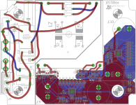
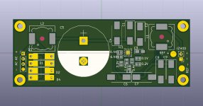
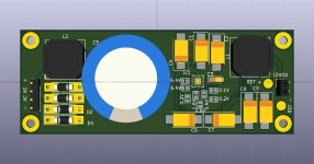
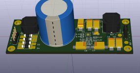
Hi Ales, your work has been a great source of inspiration to me. I have created my own board including a 2x12Vac toroid + EMI filter for mounting in a small enclosure. Maybe you (or some of the other readers) can have a look before I commit the boards to the fab. I plan to power my already finished home-made audio mixer + headphone driver which consumes +/-12Vdc @ 2x150mA.
Hi Ales, your work has been a great source of inspiration to me. I have created my own board including a 2x12Vac toroid + EMI filter for mounting in a small enclosure. Maybe you (or some of the other readers) can have a look before I commit the boards to the fab. I plan to power my already finished home-made audio mixer + headphone driver which consumes +/-12Vdc @ 2x150mA.
Attachments
Hi Ales, your work has been a great source of inspiration to me. I have created my own board including a 2x12Vac toroid + EMI filter for mounting in a small enclosure. Maybe you (or some of the other readers) can have a look before I commit the boards to the fab. I plan to power my already finished home-made audio mixer + headphone driver which consumes +/-12Vdc @ 2x150mA.
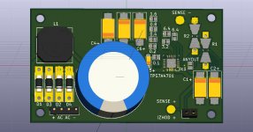
janbert, thanks for sharing your design! Coincidentally enough, I have been working on a similar design the past couple of weeks, referencing from Ales' design as well as the TI EVM and this module on ebay. I am also looking to use a Talema 70000K for an all-in-one module, but targeting the 15/25/35 VA models. I am currently fine tuning the schematic and component selection right now, but will post here once I have the PCB layout complete.
Here are some questions and suggestions I have regarding your design in comparison to Ales', others', and my own.
- Why the electrolytic and other caps on the output? I am planning on using 5x10uF X7R ceramics only on the output. All other designs I have researched followed this selection. From the TI datasheet:
Optimal noise performance is characterized using a total output capacitor value of 50 µF. Note especially that input and output capacitances must be located as near as practical to the respective input and output pin
- What type of caps are you planning on using for smoothing? I've seen in other designs ~5000uF electrolytic, followed by a 47uF tantalum (I assume to reduce total ESR?), and then the recommended 10uF X7R near the IC pads.
- Could you explain the "High freq. snubber" circuit consisting of C13/14, C15/17, and R2/3 for me? I've have not run across this in the past.
- What SMD diodes are you looking at for the rectifier? I have been trolling through Digikey and Mouser and currently Vishay's FRED Pt is the front runner. 200V, 3A, 0.93Vf and in a reasonably sized SMD package. Ales, why did you move on from the SMD bridge rectifier module from your initial designs?
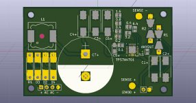
- I was going to strictly follow the central pad and via layout proposed in the datasheet (page 30). With regards to the layout of U2 in your design, without the center pad connected to the ground pour are you concerned about thermals? Further, it appears that the thermal pad is connected to the output (pin 1) on the top layer. Is this intended? From the datasheet, this pad is connected internally to GND, I am assuming this would be a short? The layout of U1 is more in line with what I would expect and was planning on implementing.
- Adding a 115/230V switch for the transformer primary wiring might make the design a bit more universal
- You might want to consider using the sense lines (pin 3) to connect at the load depending on your connection length. This seemed like a neat feature of this regulator.
If it's not obvious I've been dying to chat about this PSU / regulator implementation, good luck with your design!
Last edited:
Thanks for the great review! I am happy to take a look at your design once you are finished.
This appnote describes the snubber: http://www.ti.com/lit/an/snaa057b/snaa057b.pdf The idea is that you prevent the ringing of the diode switching.
I interpret the datasheet as ≥ 50µF. The headphone driver produces relatively big transient loads for deep basses. The bigger the buffer, and the higher the current ripple the buffer can handle (low ESR), the cleaner the bass will sound. That’s why you can buy these gold series of pro-audio capacitors which are quite expensive. From my engineering standpoint the gold capacitors are functionally equal to a big cheap electrolyte in combination with a big ceramic cap.
I have used the fastest diodes I could find at a max drop of 1V and a limited buying qty at RS components, where I have built my BOM. ES1A-E3/61T: http://www.vishay.com/docs/88586/es1.pdf
Thanks for the central pad tip! You helped me prevent a short indeed! I have modified the design according to the datasheet.
The 115Vac/230Vac option is now added by using wire bridges on the bottom side.
I was in doubt to use the sense line like proposed, because of earlier recommendations in this thread. Also the sense line could pick-up some interference of the transformer because it is a long straight antenna. If it turns out that the output ripple is not good enough, I have provided a manual solder jumper so I can bridge the sense pin to the output.
Regards, Jan Bert
Attachments
My version of supply.....any recommendation for changes?
those c6-c9 should done something with them ... why i have so big capacitors...well i gave huge roll of tantal capacitors.
If I would see Aleš pcb I woulden even bother.
Sorry Aleš. Sam če bi prej videl od tvoj izdelek bi ga naročil.
Kje si naročil pcbje?
Sem gledal nekaj ta čip in ne izgleda da se ga da vezat parallelno, ker bi rabil več toka.
Mimogrede...to je moj the first pcb")
Mej se.
Thank you
those c6-c9 should done something with them ... why i have so big capacitors...well i gave huge roll of tantal capacitors.
If I would see Aleš pcb I woulden even bother.
Sorry Aleš. Sam če bi prej videl od tvoj izdelek bi ga naročil.
Kje si naročil pcbje?
Sem gledal nekaj ta čip in ne izgleda da se ga da vezat parallelno, ker bi rabil več toka.
Mimogrede...to je moj the first pcb
Mej se.
Thank you
Attachments
By the way the inductor on the output side isn't necessary I think...
I recrate my bad design and ged rid of output inductor (was nice antena). I Add resistor R1 and R2 so it can be used in all options.
My board did work until i add load..than it crashed (was without resistors).
TO ALL : If you look datas sheet Figure 28 and figure 23 I belive on figure 28 R1 and R2 are mislabeled (R1 in place R2 and vice versa).
Any one would share som light ??
Attachments
Too bad.
I saw a nice TPS7A47 board on the Ali-market but I found no counterpart for the negative side.
So I am wondering where to get a soldered board?
Alternatively, I can place the unit on its back and solder directly on the chip. But its sure I will degrade somewhere and my way of working leads to suboptimalisation (like the story of an input inductor, or even an input capacitor that might just degrade the PSRR).
- Status
- This old topic is closed. If you want to reopen this topic, contact a moderator using the "Report Post" button.
- Home
- Amplifiers
- Power Supplies
- Low noise symmetrical PSU TPS7A4701 and TPS7A3301