I've build (breadboard) a MOSFET series regulated PSU for my 120W tube bass amp. 420 Volts, capable of 1 amp output (schematics below). I thought I had it oscilation free, but another check on my scope pointed out some issues. It's all good until ut has to supply more current (larger amp input signal), then the effect in the scope-image occurs. I can't figure out how to eliminate this oscilation. Tried to up the cap in the zobel, higher gate stopper, diode on the output, etc. The only thing that gets rid of it is to connect my scope across the speaker output! Please help, Im getting desperate.


Correct, C107 is the speedup capacitor to allow AC ripple to pass directly to the error amplifier instead of having 'to go through' R116 and R117, giving twice the amplitude and therefor better error adjustment.
But do you have any idea what could cause such an oscilation??
But do you have any idea what could cause such an oscilation??
Apart from possible stability issues, having C107 directly connected between the output and the unprotected transistor's base is quite risky: you will have problems sooner or later
Good call. Better to have a resistor in series with the base. Is there a rule of thumb for the value??
The highest value you can afford without ruining something else, but as important if not more is a B-E protection diode.Is there a rule of thumb for the value??
It is the B-E junction of Q106. It could be damaged if a transient is passed through the cap.I'm afraid I don't quite follow. Can you ellaborate on what B-E exactly and why? Thanks.
Here, it is probably better to use a diode from base to ground, it will also protect Q105 which is as vulnerable.
The series resistor will deal with the forward aspects

Cool! Thanks for the input. I asume attached image is what you suggest?
Yes
I understand R115 is intended as a gate-stopper, but a gate-stopper should be placed on the gate pin, say 220 ohms to 1K. Better to just add it.
imho R115 at 10k is high, I understand you have been increasing it. it might now create a pole too against the gate capacitance .
probably you solved it already..
imho R115 at 10k is high, I understand you have been increasing it. it might now create a pole too against the gate capacitance .
probably you solved it already..
I understand R115 is intended as a gate-stopper, but a gate-stopper should be placed on the gate pin, say 220 ohms to 1K. Better to just add it.
imho R115 at 10k is high, I understand you have been increasing it. it might now create a pole too against the gate capacitance .
probably you solved it already..
The input is still appreciated
") . The gate stopper value is something I determined by experimentation, but without actually knowing the optimum value or theoretical basis in this arrangement. I will look into it again, now the main issue is resolved.
. The gate stopper value is something I determined by experimentation, but without actually knowing the optimum value or theoretical basis in this arrangement. I will look into it again, now the main issue is resolved. The problem in this case was a loose ground connection from the output transformer's NFB due to the project being one big pile of breadboards at this moment
Ah, solder joints.
I have troubles at times, [probably] with using the correct temperature - often for speed I have it too high (300 degrees); then the flux evaporates too fast, not doing its job of binding and cleansing.
So I have to tell myself to take my time, reduce the temp.
And visual inspection with a magnifying glass .
The main role of R115 is not as a gate stopper, it should remain 10K. Its role is to protect the Rush error amplifier and the forward-biased zener in case of overdrive.The input is still appreciated
Ummm
The output voltage of this circuit is in proportion to the input voltage.
I would call it a power voltage divider not a regulator.
I have designed something very similar (560V in / 380V out) but use a couple of 200V zeners, and regulates.
The boards will arrive next week and then I will have the pleasure of looking for stability in my design.
One other thing:
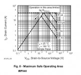
SOA of pass device.
360VAC would give you about 507V DC.
With an output of 420V DC the pass transistor would drop 87V.
I would not design with a device that I don't have information for the SOA DC limits.
The SOA for IRF840 (at least the data sheet I found) does not have this information.
Take a look at these:
http://www.toshiba.com/taec/components/Datasheet/TK12J60U.pdf
http://www.cree.com/power/products/...ia/Files/Cree/Power/Data Sheets/CMF10120D.pdf
Your call
The output voltage of this circuit is in proportion to the input voltage.
I would call it a power voltage divider not a regulator.
I have designed something very similar (560V in / 380V out) but use a couple of 200V zeners, and regulates.
The boards will arrive next week and then I will have the pleasure of looking for stability in my design.
One other thing:
SOA of pass device.
360VAC would give you about 507V DC.
With an output of 420V DC the pass transistor would drop 87V.
I would not design with a device that I don't have information for the SOA DC limits.
The SOA for IRF840 (at least the data sheet I found) does not have this information.
Take a look at these:
http://www.toshiba.com/taec/components/Datasheet/TK12J60U.pdf
http://www.cree.com/power/products/...ia/Files/Cree/Power/Data Sheets/CMF10120D.pdf
Your call
Attachments
It does actually regulate, not very tightly perhaps and it will have a negative tempco, but it is not a mere divider.Ummm
The output voltage of this circuit is in proportion to the input voltage.
I would call it a power voltage divider not a regulator.)
Ummm
The output voltage of this circuit is in proportion to the input voltage.
I would call it a power voltage divider not a regulator.
I have designed something very similar (560V in / 380V out) but use a couple of 200V zeners, and regulates.
The boards will arrive next week and then I will have the pleasure of looking for stability in my design.
Look again, it is a regulator (feedback). T101/T102/R107 is a CCS for the resisor network R108 to R111, giving a fixed voltage for the differential amp T105/T106, which is also fed through a CCS, both for stability reasons. The output is is fed through the symmetrical voltage divider (R116 to R119) to the other end of the diff. amp. This arrangement gives a regulated output of twice the voltage present at T105. Not super tight as Elvee pointed out (an opamp as the diff amp would e.g. give better results), but for my intends an purpose it's more than enough. I've also build a regulator with zener reference, but found this design to preform better.
Those are some nice pass devices. But I wouldn't worry to much about the DC SOA, it's more a question of power dissipation given the current drawn and voltage dropped across it. In the IRF840's case it's 125W. With a max current of around 800mA and the voltage dropped around 85V, I'm well within this limit (68W).One other thing:
SOA of pass device.
360VAC would give you about 507V DC.
With an output of 420V DC the pass transistor would drop 87V.
I would not design with a device that I don't have information for the SOA DC limits.
The SOA for IRF840 (at least the data sheet I found) does not have this information.
Take a look at these:
http://www.toshiba.com/taec/components/Datasheet/TK12J60U.pdf
http://www.cree.com/power/products/...ia/Files/Cree/Power/Data Sheets/CMF10120D.pdf
Your call
Last edited:
- Status
- This old topic is closed. If you want to reopen this topic, contact a moderator using the "Report Post" button.
- Home
- Amplifiers
- Power Supplies
- Series MOSFET regulator 400V, what the hell