Hi All,
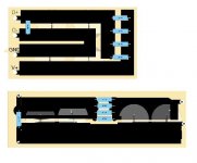
Here is PCB that I will use for Aleph 30
My questions are
1. PCB trace is about 5 mm is that ok?
2. Input and out voltage is close, is that ok? ussually I seen Input voltage on one side and the out put is on the other side
let me know please....
Here is PCB that I will use for Aleph 30
My questions are
1. PCB trace is about 5 mm is that ok?
2. Input and out voltage is close, is that ok? ussually I seen Input voltage on one side and the out put is on the other side
let me know please....
Attachments
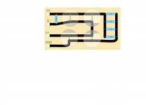
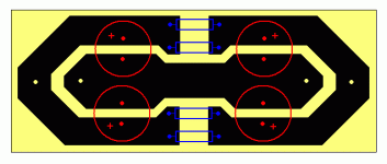
Are the labels correct? You seem to have D- connected to V+.
Yeah you are right.... supposedly the other way around
Why not use more copper? e.g. Thicken the V+ and D+ tracks and fill in the whole center area between GND and D-. It doesn't cost any extra. In fact if you're etching you're own boards, it saves money.Corrected
P.S. Are those resistors supposed to be 0.47 Ohms? Seems too low for effective filtering.
You just have to be careful that ground currents from charging pulses don't end up in the wrong place. Leaving the ground trace as a line rather than an area maintains the clear distinction between PSU input from rectifier (dirty) and PSU output (clean). Then the clean end can go to the signal ground without injecting buzz.godfrey said:Thicken the V+ and D+ tracks and fill in the whole center area between GND and D-.
I got what you are sayingYou just have to be careful that ground currents from charging pulses don't end up in the wrong place. Leaving the ground trace as a line rather than an area maintains the clear distinction between PSU input from rectifier (dirty) and PSU output (clean). Then the clean end can go to the signal ground without injecting buzz.
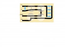
Maybe this one is better?
Attachments
Why not use more copper? e.g. Thicken the V+ and D+ tracks and fill in the whole center area between GND and D-. It doesn't cost any extra. In fact if you're etching you're own boards, it saves money.
P.S. Are those resistors supposed to be 0.47 Ohms? Seems too low for effective filtering.
What value you are suggesting for the resistor?
Yes, but it still needs more copper. You're etching away all the good stuff.Maybe this one is better?
No suggestion, I was just surprised at the value. If that's what Nelson suggests, I certainly won't argue.What value you are suggesting for the resistor?
Yes, but it still needs more copper. You're etching away all the good stuff.
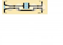
What about this??
Attachments
No different. I didn't mean 'straight line', just a line as you originally had. The idea is simply to maintain the difference between PSU input (from rectifier) and output (to circuit). It doesn't matter if these are physically close to each other as long as the currents are forced to go where you want them to. You could just do a maximum copper layout with a cut along the middle to separate the in and out currents.tony Ma said:Maybe this one is better?
You've still got a skinny ground track. I was thinking of something more like this (but neater).What about this??
Attachments
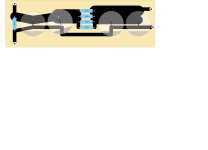
post12.
the lower version has a loop area that emits emf when the current varies.
The upper version has a lloop area in the lower half and that emits emf when the current changes. The upper half also has loop area that emits emf when the current changes.
BUT, !!!!!!!!!
the two loops are out of phase. The lower loop area cancels the upper loop area, leaving just the end area and the input/output terminals to have loop area to cause interference.
No different. I didn't mean 'straight line', just a line as you originally had. The idea is simply to maintain the difference between PSU input (from rectifier) and output (to circuit). It doesn't matter if these are physically close to each other as long as the currents are forced to go where you want them to. You could just do a maximum copper layout with a cut along the middle to separate the in and out currents.
Noted, now I learned some thing new again tks.....
post12.
the lower version has a loop area that emits emf when the current varies.
The upper version has a lloop area in the lower half and that emits emf when the current changes. The upper half also has loop area that emits emf when the current changes.
BUT, !!!!!!!!!
the two loops are out of phase. The lower loop area cancels the upper loop area, leaving just the end area and the input/output terminals to have loop area to cause interference.
So what you are suggesting?
Disagree. The current in the two loops is different, so the EMI won't cancel.the two loops are out of phase. The lower loop area cancels the upper loop area, leaving just the end area and the input/output terminals to have loop area to cause interference.
@tony Ma:
6L6 raised a worrying point - are you sure this is the right sort of PSU for the Aleph? Also, I don't know what value resistors to recommend as I don't know anything about the Aleph.
Re:
One could do something like this, but I don't know if it's worth it. Cancellation will only be good at a distance large compared to the distance between the loops. The ideal solution would be to use double-sided PCB and have the forward and return current paths directly above and below each other.The lower loop area cancels the upper loop area...
Attachments
Re:
One could do something like this, but I don't know if it's worth it. Cancellation will only be good at a distance large compared to the distance between the loops. The ideal solution would be to use double-sided PCB and have the forward and return current paths directly above and below each other.
I am a newbee.... and I am planning to make my own PCB seems it is hard to make 2 layers PCB
Yes there should be bipolar PS. I am thinking to make separate
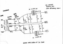
here is the complete sets.
Attachments
No need for a 2 layers PCB. In fact the layouts you posted should work fine. The rest of us are just nit-picking. You ask for opinions - you get opinions.I am a newbee.... and I am planning to make my own PCB seems it is hard to make 2 layers PCB

OK that makes sense, and looks good. I like where you've connected ground (after the filtering).Yes there should be bipolar PS. I am thinking to make separate
here is the complete sets.
- Status
- This old topic is closed. If you want to reopen this topic, contact a moderator using the "Report Post" button.
- Home
- Amplifiers
- Power Supplies
- Need opinion