Hey Guys,
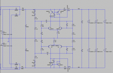
I've been working on an active power filter for an amp I'm designing: Think Bybee Music rail.
This one is pretty simple, but offers exceptional ripple rejection with a low drop.
Using low Rds P-ch MOSFET and a pair each of 2N5551 and 2N5401, the results have me quite excited to build it up. The model I'm running has given me around 2mV total ripple with an output current draw of up to 12A peaks. The load current sources are a fixed 6A, a 3A @ 20Hz, 3A @ 1000Hz. I don't have a spice model for the IRF5210 so I substituted the Siliconix Si7469DP which seems to offer similar characteristics. The negative rail compliment uses a low Rds N-ch.
Here's a few shots of the simulation showing both the total ripple with current as well as the unfiltered and filtered voltage for comparison. Ripple has been reduced by a factor of just over 1000, or a little more than 63dB. Total dissipation in the MOSFET is around 15W with average delivered power of nearly 400W.
I honestly can't say if this has been done, but it's probably not new. I'm very pleased with the results as you can probably tell.
Attachments
Last edited:
2mv of ripple with 12A peaks is very impressive! and it looks like you are only sacrificing about 2V to do it too.")
Tony.
2V was the target. If you remove 1 of the diodes feeding R4 and R9, you can get even less overall drop. But that does result in an increase in ripple when a full 12A peak 20Hz modulation is employed. In reality, such a demand on an amp would be exceedingly rare, so a single diode would probably be more than adequate for music signal loads into 8 Ohm.
Here's a shot simulating full power 20Hz into an 8 Ohm load and a single diode feeding R4.
Attachments
Last edited:
That could be quite a handy circuit if it performs as simulated. I have used the the LT1085 before for similar purposes but it only goes to 7A
The IRF3210 and IRF3415 can handle 40A with a 200W power rating (given adequate heat sinking of course). This set up should be able to clean up virtually any power amp supply you could think of. Parts cost is very reasonable.
JLH Ripple Eater?
The ripple eater is a shunt type regulator, and from what I have read so far, is limited to about 5 Amp. I'm not sure about its suitability for something as drastic as taking care of the ripple voltage of an unregulated PSU like that of an amplifier, or the large variation in current that would need to be supplied to an amplifier under load.
Also, based on the values of the feedback components, I'm not so sure that the Ripple Eater would have as high a rejection for rail variations as this one.
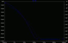
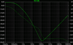
Here's a shot of the transfer function of output ripple/input ripple. This does a serious job of attenuation over the frequency range where current draw is highest via music power (below 300Hz) which creates the largest ripple levels on the main filter caps.
Adding a shunt regulator to this one for high frequencies may be beneficial though. I may have to break out LTSpice and do just that.
Attachments
I honestly can't say if this has been done, but it's probably not new. I'm very pleased with the results as you can probably tell.
Interesting design! Somewhat similar to AMB's a22 The σ22 Regulated Power Supply but you have some new good stuff in there. You've eliminated the zener in the voltage reference (I'm assuming the 1N4148s are less noisy than the zener, but haven't checked specs), have the mosfets turned the other way for a LDO rather than source-follower, and your positive and negative halves are completely independent. I especially like that last point since that issue makes troubleshooting the a22 a little harder - when one rail goes in a certain way they both go. Probably no pressing need for the mosfets to be configured as source-follower since the reference voltage for the error amp is sampled after the mosfets in both designs.
But I do like AMB's idea of feeding the voltage reference parts with the separate cap multiplier to create clean(er) power from the main rail, at the expense of a couple of volts. Especially in the case of really large currents moving through the main rails (and associated IR rail ripple), which both designs can handle. I've suggested to AMB before of connecting the cap multiplier(s) to the main rail through an inductor to help nuke any any frequency noise that otherwise would zoom right through the cap mults. Also beefing up the cap mult transistors to BD139/140 and putting a reverse diode across the BE junction given the caps on either side. I also like how AMB has actual current sources feeding the LTPs, rather than the (16k) resistors, for higher impedance looking back in. Those current source diodes are getting scare and pricey though. Probably better at this point to use a depletion mosfet or BJT based ccs.
Last edited:
agdr.
Thanks for pointing out the Sigma22. Very similar circuit topology for sure. But unlike the Sigma22, this unit is not regulated. The diodes act as a fixed voltage drop to allow the reference voltage to track the average voltage on the main filter caps. This allows the MOSFET to maintain a fairly constant 2V drop, minimizing power lost in the device. The way the circuit is designed, it is basically acting as a 2nd order lowpass filter with unity gain. As the input level changes slowly, the output will track. But higher frequency variation, like rectifier ripple, is filtered out. It's sort of an active version of a CRC supply with much higher rejection capability in the frequency range where most power will be drawn from the supply (below 400Hz).
I'm still evaluating its performance as load current frequency exceeds 1000Hz. Seems fine so far as long as the current levels are not too high, but I have noticed at high power levels above 2000Hz that output ripple is reaching into the 100mV range. And if there is too much capacitance on the output, it seems to make it more difficult to keep ripple levels very low. I'm looking to improve the output impedance over a broader frequency range.
~60dB is comparable to commercial LDOs (except they regulate as well; suppose you could get a low voltage one and bias it up to some fraction of Vin to use it for filtering). I'm guessing the higher frequency performance isn't as good, i.e., you wouldn't get away with it on a switching supply.
Two things bound such a design: 1. as the MOSFET saturates (voltage drop gets near the minimum of Rds(on) * Id), transconductance drops sharply and isolation similarly disappears. In this regime, you depend entirely on the performance of the driver/amplifier to cover low frequency response. 2. But that amplifier must be compensated at high frequencies, else it's just a big oscillator. So you might get, say, 100dB at 1Hz, but it's already tapering off by 60Hz (as shown, overall gain is probably more like 60dB, which is about your measured attenuation, so the cutoff frequency is probably a smidge over 100Hz), dropping to nil at fT (maybe a few hundred kHz). 3. A corollary to these: because the gain changes rapidly in saturation, compensation must also change, or be overcompensated enough to keep things in check. This can hurt performance further. (The high-voltage-drop case should really be worst case, but do remember to check it in all conditions, in any case! It's very easy to ignore low-line and startup conditions in simulations.)
Incidentally, for simulation purposes, there's no need to generate 17 painstaking seconds of data waiting for sources to stabilize -- just use a DC source with AC ripple superimposed. Use an AC (small signal) analysis to check the rough frequency response (being sure to check the DC operating points, of course).
The load you use is also noteworthy: it's true that, for a small change, almost any load looks like a current source, but since you're looking at small changes in current AND voltage, it still matters whether it's a resistor, current sink or what. Now, a solid state amplifier *does* tend to look like a current sink -- but I'm not going to make that assumption, because if you need this much filtering, your circuit's PSRR must be poor to begin with, or your signals very small. In either case, check for best results!
Tim
Thanks for the thoughtful reply.
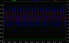
Here's a shot of the transfer function showing the 0dB rejection at DC (LDO output tracks average line level) with maximum attenuation at just over 100Hz and then slowly rising after that. But there's still 40dB attenuation of 10KHz input noise on the output. This transfer function is with a typical ampilfier load at idle (500mA bias draw).
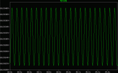
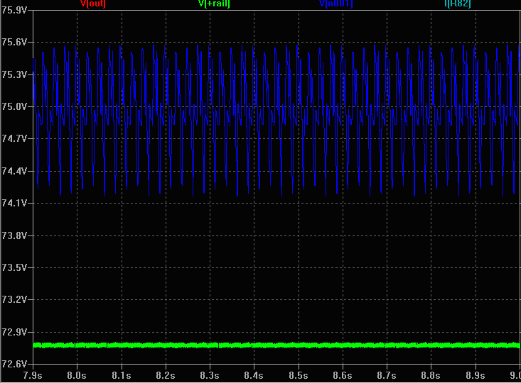
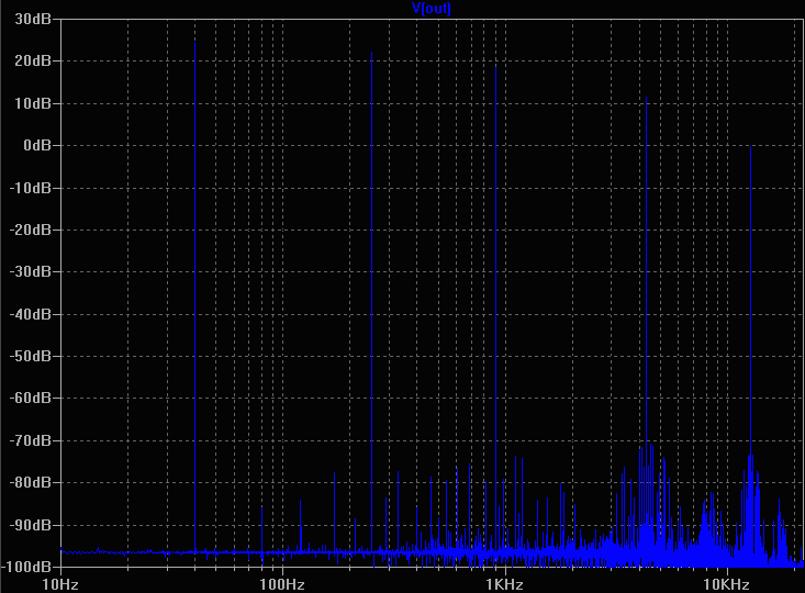
I'm using a MOSFET with Rds at full on that won't exceed .06 Ohm. Even with 15A peak draw, the device won't be dropping even 1V. The only time the device would ever see that kind of current draw would be with 4 Ohm loads pulling 500W, which will be exceedingly rare. Even then, all that happens is the device simply acts as a .06 Ohm resistor for the duration of the peak current draw. During the amplifier operation in Class B, when the positive current draw goes to 0, there is some overshoot on the LDO recovery. I've included some other shots showing the input ripple using an AC source of 1V@120Hz and 70V offset, and .15 Ohm source impedance. The load is an amp using a multitone music simulation signal. The closeup of the LDO output looks a bit hairy, but in reality, the levels are quite small. I've included a spectral content of the rail under load as well. The two spikes you see are part of the test signal fed to the amplifier load. The spurious stuff is over 100dB below the output signal level (20dB).
The amp circuit I will be pairing with this LDO already has PSRR of around 80dB at 120Hz. Increasing that to a total of 120dB or more doesn't seem like a waste of time if you're trying to make the quietest amp you can, especially for use with high sensitivity speakers.
Here's a shot of the transfer function showing the 0dB rejection at DC (LDO output tracks average line level) with maximum attenuation at just over 100Hz and then slowly rising after that. But there's still 40dB attenuation of 10KHz input noise on the output. This transfer function is with a typical ampilfier load at idle (500mA bias draw).
I'm using a MOSFET with Rds at full on that won't exceed .06 Ohm. Even with 15A peak draw, the device won't be dropping even 1V. The only time the device would ever see that kind of current draw would be with 4 Ohm loads pulling 500W, which will be exceedingly rare. Even then, all that happens is the device simply acts as a .06 Ohm resistor for the duration of the peak current draw. During the amplifier operation in Class B, when the positive current draw goes to 0, there is some overshoot on the LDO recovery. I've included some other shots showing the input ripple using an AC source of 1V@120Hz and 70V offset, and .15 Ohm source impedance. The load is an amp using a multitone music simulation signal. The closeup of the LDO output looks a bit hairy, but in reality, the levels are quite small. I've included a spectral content of the rail under load as well. The two spikes you see are part of the test signal fed to the amplifier load. The spurious stuff is over 100dB below the output signal level (20dB).
The amp circuit I will be pairing with this LDO already has PSRR of around 80dB at 120Hz. Increasing that to a total of 120dB or more doesn't seem like a waste of time if you're trying to make the quietest amp you can, especially for use with high sensitivity speakers.
Attachments
Thanks for the thoughtful reply.
Here's a shot of the transfer function showing the 0dB rejection at DC (LDO output tracks average line level) with maximum attenuation at just over 100Hz and then slowly rising after that. But there's still 40dB attenuation of 10KHz input noise on the output. This transfer function is with a typical ampilfier load at idle (500mA bias draw).
I'm using a MOSFET with Rds at full on that won't exceed .06 Ohm. Even with 15A peak draw, the device won't be dropping even 1V. The only time the device would ever see that kind of current draw would be with 4 Ohm loads pulling 500W, which will be exceedingly rare. Even then, all that happens is the device simply acts as a .06 Ohm resistor for the duration of the peak current draw. During the amplifier operation in Class B, when the positive current draw goes to 0, there is some overshoot on the LDO recovery. I've included some other shots showing the input ripple using an AC source of 1V@120Hz and 70V offset, and .15 Ohm source impedance. The load is an amp using a multitone music simulation signal. The closeup of the LDO output looks a bit hairy, but in reality, the levels are quite small. I've included a spectral content of the rail under load as well. The two spikes you see are part of the test signal fed to the amplifier load. The spurious stuff is over 100dB below the output signal level (20dB).
The amp circuit I will be pairing with this LDO already has PSRR of around 80dB at 120Hz. Increasing that to a total of 120dB or more doesn't seem like a waste of time if you're trying to make the quietest amp you can, especially for use with high sensitivity speakers.
I just got through a simulation that increased the bias current in the differential pair and it definitely improved the recovery of the MOSFET from the no-current to on-condition. I'll post an update to the configuration after I've played around some more.
Last edited:
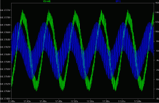
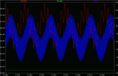
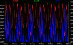
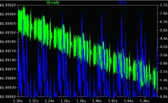
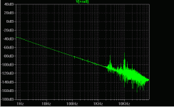
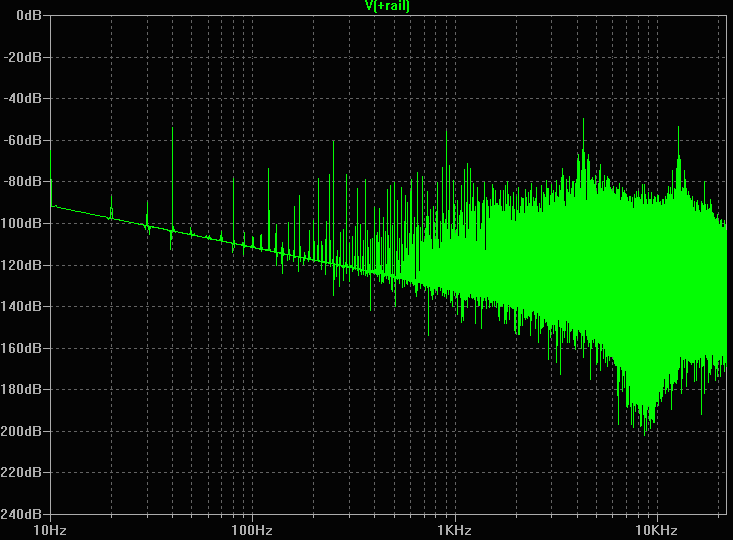
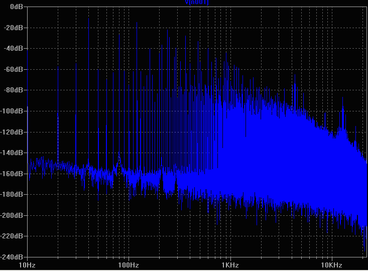
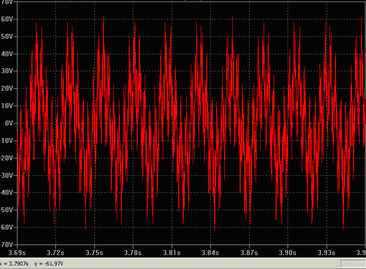
OK, some progress and a thorough simulation. The power supply is fed with full bridge rectifier and AC voltage sources. The amplifier is fed with a 5 tone test signal simulating a real world music signal. Peak output power into 4 Ohm load resulting in 930W instantaneous peaks and and 15A peak current through the LDO.
The pictures show spectral content of the amp output, the LDO rail, and the rectifier side of the LDO. Also shown are the input and output of the LDO in the time domain as well as a shot of the amp output signal.
It appears that the use of the LDO greatly cleans up the power rail, far more than even doubling the rectifier cap bank would do at a much lower cost. This simulation is done with 30,000uF on the rectifier filter and 6000uF on the LDO output.
- Status
- This old topic is closed. If you want to reopen this topic, contact a moderator using the "Report Post" button.
- Home
- Amplifiers
- Power Supplies
- Low Drop Out Power Rail Filter