Here is a small lab supply project.
It is very basic yet complete, and has many desirable features that simple projects based on 317 or 723 lack:
-Voltage and current variable from zero to the maximum without swiching.
-Uses very few and common discrete components: 4 small signal transistors, one medium power and the power ballast, plus two or three caps and a pinch of resistors.
-No auxiliary supply required
-Since it is discrete-based, voltage and current ranges can be chosen freely, without the voltage restrictions usually associated with ICs
-On/Standby switch, and visual indication of the current mode
-Low drop-out architecture meaning it's, ...well, low drop-out obviously, which is good for an effective utilization of the transformer, but also that it is inherently a current regulator servoed into voltage and it can react very quickly to overcurrents. This, coupled with a minimal output capacitance means a very good protection for the tested circuits.
-Stable to within millivolts for line and load regulation, and good temperature stability. Not metrology grade, obviously, but quite sufficient for workshop use, ideal for beginners.
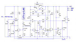
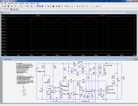
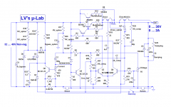
Here is the schematic, dimensioned for a very classical 0-30V, 0-2A.
Some details and pics will follow.
It is very basic yet complete, and has many desirable features that simple projects based on 317 or 723 lack:
-Voltage and current variable from zero to the maximum without swiching.
-Uses very few and common discrete components: 4 small signal transistors, one medium power and the power ballast, plus two or three caps and a pinch of resistors.
-No auxiliary supply required
-Since it is discrete-based, voltage and current ranges can be chosen freely, without the voltage restrictions usually associated with ICs
-On/Standby switch, and visual indication of the current mode
-Low drop-out architecture meaning it's, ...well, low drop-out obviously, which is good for an effective utilization of the transformer, but also that it is inherently a current regulator servoed into voltage and it can react very quickly to overcurrents. This, coupled with a minimal output capacitance means a very good protection for the tested circuits.
-Stable to within millivolts for line and load regulation, and good temperature stability. Not metrology grade, obviously, but quite sufficient for workshop use, ideal for beginners.
Here is the schematic, dimensioned for a very classical 0-30V, 0-2A.
Some details and pics will follow.
Attachments
Thanks.Awesome. Especially the single supply requirement makes this a very nice one.
is the qtlp690c chosen with a reason or will any blue/white led do?
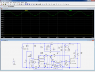
It also works with a white or blue LED without modification, see simulable file.
Anyway, it can be made to work with any LED or combination having >3.6Vf: you just need to use 5V6, 6V2 or more for D4.
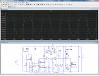
Note: in the sim, parameters I & V set the current and voltage potentiometers settings, value comprised between 0 and 100%
Attachments
The current mode operation of the ballast also has another interesting byproduct: the circuit is relatively immune to the effects of the power wiring: to the ballast, and from the non-regulated input.
The peculiar voltage control gives a ~semi-log-like feel when using the pot.
It makes the accurate adjustment of low voltages easy without resorting to a separate fine adjustment control.
The overcurrent indication is relatively "soft", because of the relatively low gain of the single transistor.
It also gives a hint of "advance warning": the LED begins to glow before the limitation actually enters into action.
These parameters, advance, sharpness or softness can be adjusted by modifying R23 and D6.
A compensation network is fitted to the current regulator. In reality, it is not required: my prototype remains unconditionally stable without it, but it looks necessary in sim, I have therefore included it.
R19 compensates the residual internal resistance of the supply. There too, the reality is better than the sim: the sim requires 12K as optimum value, against 27K in reality.
When the supply is adjusted to zero and left open circuit, a voltage of ~0.5V appears at the output. It is caused by the bias potentials that are reinjected through R15.
The 1K bleeder limits this voltage but its presence is required to keep good dynamic performance at low loads, not by this effect, and reducing it further would waste power.
Anyway, the source impedance of this 0.5V is ~5K, and it falls as soon as a load is connected.
It is a (small) price to be paid for the simplicity and performance of the circuit.
To make the zero coincide exactly with the mechanical zero of the pot, a trim resistor has to be added in // with R11. On my prototype, it is 15K, but it depends on the actual value of the voltage potentiometer.
Attachments
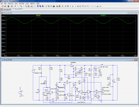
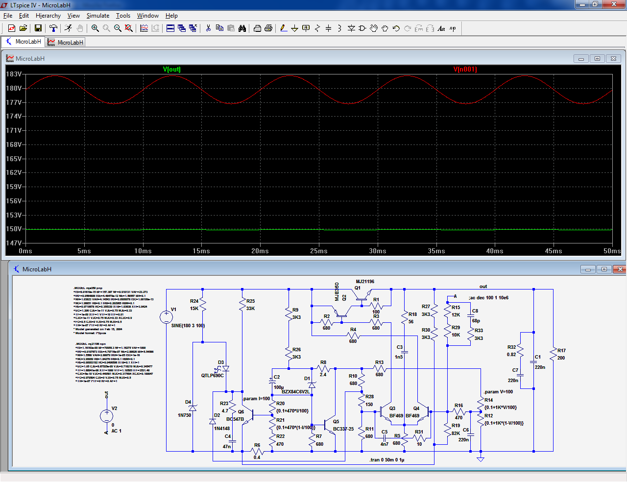
Here is an example showing how this supply can be formatted for a custom range: in this case, 150V/1A.
Further optimizations would be possible, to reduce the quiescent power amongst other things, and in practice, more than one ballast should be used, but it illustrates the versatility and portability of the concept.
Further optimizations would be possible, to reduce the quiescent power amongst other things, and in practice, more than one ballast should be used, but it illustrates the versatility and portability of the concept.
Attachments
Even more intriguing, thanks to its symmetrical nature the circuit also accepts (almost) transparently a NMOS.
There would be some restrictions on the range of the output voltage, but for a HV supply this would be a minor inconvenient.
Note that none of the above variants has been actually tested.
There would be some restrictions on the range of the output voltage, but for a HV supply this would be a minor inconvenient.
Note that none of the above variants has been actually tested.
Attachments
Here is an update on this project:
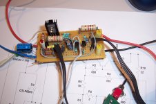
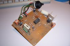
I have installed the supply circuit in its "target", a clumsy old EA3013 30V/5A supply from Elektro-Automatik (see a pic of the control board below).
This supply was rather appalling, and I used it very rarely, only as a last resort, when all the rest was already in use.
It is a crude 723-based design, with some "trick" to reach 0V, and it is unstable, noisy, and impractical with the current control in three discrete steps beginning at 0.5A. Not the finest piece of electronic gear, even for very basic workshop use.
I simply removed the control board, and kept the case, meter, transformer, rectifier, and power circuitry which were of acceptable quality.
I also kept the automatic 15/30V transformer switching board.
I had some adaptations to make to have everything working properly.
First I noticed that the current control didn't go exactly to zero. The remedy was simple: I just had to replace Q6 by a BC337, same type as Q5. I don't know how I could miss that, it is obvious that using different types would introduce an offset.
With a BC337, the control goes down to a few mA.
Under some conditions, I also had a HF oscillation in voltage mode.
The reason was the output wiring, daisy-chained from the ballasts, to the output via the ammeter, and back to the board with bypass caps both on the board and across the output terminals.
Combined with the wiring, this resulted in two second order filters cascaded, a bit too much for the stability of the loop. I simply had to connect the compensation network R18/C3 to the emitter of the ballast.
Then, I noticed that with a 5A load, the non-regulated voltage was 41V.
The 723 needed a lot of headroom, but with this board, I could comfortably and safely reach 36V. I added a 1K trimmer in series with R15, and also corrected R11 with a 100 ohm series resistor.
That's it: now, the supply has controls for 0-36V and 0-5A that are smooth as silk, a standby switch and a current mode indication.
It is also quiet and stable, and the single voltage control is much more convenient than the original "Gross/fein" pots, and is as accurate thanks to the quasi-log feel.
This doesn't make it a high end supply, but now it is at least decent and usable.
Attachments
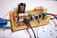
i'm (when i feel like i've earned a break) working on a PCB.
Since i'm doing this for the first time following a different strategy than i'm used to (in/out on same side, path folded in U shape and defined ground return paths instead of super-short paths and a ground plane) it will take a while. also maybe a little because of exams@school.
where do you measure I? R6?
Last edited:
“ I just had to replace Q6 by a BC337, same type as Q5“
“ I simply had to connect the compensation network R18/C3 to the emitter of the ballast.”
“ I added a 1K trimmer in series with R15, and also corrected R11 with a 100 ohm series resistor.”
“now, the supply has controls for 0-36V and 0-5A that are smooth as silk, a standby switch and a current mode indication.” It was 0-30vdc and 2A.
“the single voltage control is much more convenient than the original "Gross/fein" pots”
This is a very nice project, but I am having trouble following some of this. Are these mods you made to your original schematic? If so can you modify the original schematic and repost it.
I am also wondering how that “automatic 15/30V transformer switching board" works. As you increase the voltage from 0 to 36vdc, it must sense the output voltage and then at the right time switch from 15v to 30v. But as it switches do the relays momentarily give zero voltage, as in 15v zero for a fraction of a second and then 30v.
Yes.i'm (when i feel like i've earned a break) working on a PCB.
Since i'm doing this for the first time following a different strategy than i'm used to (in/out on same side, path folded in U shape and defined ground return paths instead of super-short paths and a ground plane) it will take a while. also maybe a little because of exams@school.
where do you measure I? R6?
If you make a PCB, it is probably a good idea to include all the options, to maximize its flexibility and fully benefit of its versatility.
I will redraw a suitable schematic.
The topic has in fact two parts: the first deals with the presentation of a simple supply concept, illustrated with an example having numerical values, and the second shows a practical application, the replacement of the control board in an existing supply.This is a very nice project, but I am having trouble following some of this. Are these mods you made to your original schematic? If so can you modify the original schematic and repost it.
I understand that this can lead to some confusion, especially since the "general" circuit is so much like the application example.
That's no coincidence of course: when I designed the circuit, I had in mind that particular application.
I first had to build my prototype as a stand alone supply, to make sure it was proper and healthy before I could blend it with the existing circuits, otherwise, in case of problems I wouldn't have any reference point and would have had diificulty tracing the origin of problems.
As I said above, I will post a more general schematic, including all the options and mods.
At present, all the correctives except for Q6 apply to the particular issues arising from grafting the circuit onto an existing supply.
The original supply was equipped with a very common accessory, a voltage-sensing relay to switch the transformer's winding when the output voltage is below 15V, to reduce the dissipation in the ballast. I kept this part almost unchanged.I am also wondering how that “automatic 15/30V transformer switching board" works. As you increase the voltage from 0 to 36vdc, it must sense the output voltage and then at the right time switch from 15v to 30v. But as it switches do the relays momentarily give zero voltage, as in 15v zero for a fraction of a second and then 30v.
The switchover time is short enough to allow the filter cap to ride through, as rikkitikkitavi rightly remarks:
I see no switch/relay or sensing circuit in the posted schematic, so I assume this is done on AC side of the rectifier, i e a transformer with two windings. That would of course prevent any voltage dip, given that the rectifier caps are large enough.
Last edited:
I am pretty sure it can: I have successfully simulated some examples, see above, BUT simulation is no substitute for reality, especially in the high voltage field.Hey
Can this schematic work for higher voltage?
I am 99.9% confident I could have a high voltage version working, but realistically the working sim schematic would probably need some tweaking and adaptations to be really safe and effective in reality.
I will probably test a HV version in the coming days or weeks (or months).
In the mean time, if you have sufficient experience with HV, you can try it (carefully) for yourself.
I made a quick and dirty breadboard test of this HV version:
It worked immediately (except I had connected the 330µF/400V filter cap in reverse and had a narrow escape).
There are some differences with the schematic: transistor types were different, with a 2SC2922 as a ballast for example, but that is secondary.
In order to reduce the quiescent dissipation, I also doubled the values of all DC-affected resistors: for example, R9 & 26 became 6.8K, the 680 ohm became 1.2K, the voltage and current pots became 2.2K and 1K, etc.
That is acceptable since the output current is half of the low-voltage version.
In order to keep some advance warning with the current limit, I changed D4 for a 5V6, and the optimum output resistance compensation R19 was 22K, but this did not affect the functionnality of the supply, and at all times it was stable both in current and voltage modes, despite the breadboarding.
Thus, it looks pretty safe.
For this kind of voltage, it essential to keep in mind the SOA limits of the pass element(s).
Neglecting that will certaily result in molten silicon.
I also dropped in a 2SK794 NMOS as a replacement for Q1, and it worked transparently, with just R1 raised to 680ohm. All the parameters remained unchanged, including the compensation resistor.
I even played the sorcerer's apprentice by removing completely the compensations C3 and C5, and it remained stable, both in voltage and current, but I don't recommend it, as they look necessary in the sim.
Last edited:
ELvee, I looked over your post 13 were you posted your latest schematic. I noticed that you left several values off of the schematic. Was this an over sight or are we supposed to calculate these for our specific use?
Components with no values.
R32, R28, R26, R29, C8, R17, R20, D1, C7, R21, R30, R31, C10.
Should Zero adjust R and I Adj, be a resistor or a POT?
Thanks
Components with no values.
R32, R28, R26, R29, C8, R17, R20, D1, C7, R21, R30, R31, C10.
Should Zero adjust R and I Adj, be a resistor or a POT?
Thanks
These are optional components you have to use (and dimension) in specific cases.ELvee, I looked over your post 13 were you posted your latest schematic. I noticed that you left several values off of the schematic. Was this an over sight or are we supposed to calculate these for our specific use?
Components with no values.
R32, R28, R26, R29, C8, R17, R20, D1, C7, R21, R30, R31, C10.
Should Zero adjust R and I Adj, be a resistor or a POT?
Thanks
For example, with a higher voltage version, it is convenient to split the dropping resistors in two or three to spread dissipation, and it is possible to add supplementary filtering in the middle, etc.
You pick and choose want you want, and calculate it accordingly.
The latest 150V 1A example uses some of these options.
You won't find a pot for the Iadj resistor, it will be a few ohm, and anyway, additional resistors are much more stable than pots. That's slightly more inconvenient, but once it's done, you gain peace of mind, it doesn't vary anymore.Should Zero adjust R and I Adj, be a resistor or a POT?
Last edited:
- Home
- Amplifiers
- Power Supplies
- Lab supply on a shoestring