Hi all,
Having picked up a used spectrum/network analyser just recently in a moment of big luck, I thought I'd share any meaningful measurement I'm doing with it, over time. Not many people will have access to such an instrument, let alone hobbyists, and measurements of power supply components and systems are scarce.
A network analyser is an extremly poweful tool for impedance measurements which is basically most what power supply issues are about. Looking at the effective impedance seen at the point of load, say, a chip amp's power pins, is what counts, effectively.
The spectrum/network analyser was built late '90ies by the reputed german measurement equipment company Wandel & Goltermann.
The model is SNA-2, the second model in their range which adds phase measurement capability to the earlier SNA-1. Frequency range is 100Hz...180MHz which is just perfect for audio use.
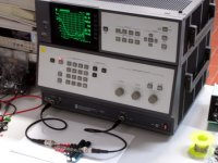
Sitting on my bench it looks like this (note that it is comprised of two really heavy 19" die-cast aluminum boxes packed with electronics to last cubic inch) :
Having picked up a used spectrum/network analyser just recently in a moment of big luck, I thought I'd share any meaningful measurement I'm doing with it, over time. Not many people will have access to such an instrument, let alone hobbyists, and measurements of power supply components and systems are scarce.
A network analyser is an extremly poweful tool for impedance measurements which is basically most what power supply issues are about. Looking at the effective impedance seen at the point of load, say, a chip amp's power pins, is what counts, effectively.
The spectrum/network analyser was built late '90ies by the reputed german measurement equipment company Wandel & Goltermann.
The model is SNA-2, the second model in their range which adds phase measurement capability to the earlier SNA-1. Frequency range is 100Hz...180MHz which is just perfect for audio use.
Sitting on my bench it looks like this (note that it is comprised of two really heavy 19" die-cast aluminum boxes packed with electronics to last cubic inch) :
Attachments
The little test jig I made for capacitor etc measurement :

A short coaxial cable was cut in the middle and a tiny double-size blank PCB was soldered in between, forming a tiny capacitor (a few pF at most).
One end of the coax was fed by the tracking generator of the analyser while the other end goes directly to the receiver input. System impedance is 75R. When a DUT (Device Under Test) is low impedance, fractions of an ohm typically compared to the system impedance this forms a constant current source and the voltage seen at the output is proportional to impedance of the DUT.
Plotting the transfer function of the jig alone looks like this :

We can see a pretty perfect line at 0dB with a slight roll-off at the highest frequencies (above 40MHz) coming from the tiny capacitance mentionened and other high-freq effect in the measurement chain. Horizontal scale is ranging 6 decades from 100Hz to 100MHz, in 1-2-4-8 increments for the grid lines (as indicated). This setting is kept for the rest of todays measurements.
A short coaxial cable was cut in the middle and a tiny double-size blank PCB was soldered in between, forming a tiny capacitor (a few pF at most).
One end of the coax was fed by the tracking generator of the analyser while the other end goes directly to the receiver input. System impedance is 75R. When a DUT (Device Under Test) is low impedance, fractions of an ohm typically compared to the system impedance this forms a constant current source and the voltage seen at the output is proportional to impedance of the DUT.
Plotting the transfer function of the jig alone looks like this :
We can see a pretty perfect line at 0dB with a slight roll-off at the highest frequencies (above 40MHz) coming from the tiny capacitance mentionened and other high-freq effect in the measurement chain. Horizontal scale is ranging 6 decades from 100Hz to 100MHz, in 1-2-4-8 increments for the grid lines (as indicated). This setting is kept for the rest of todays measurements.
Using a 0.1R resistor as a reference to adjust vertical dB scale to read in dB ref. 1 Ohm :

Resulting impedance plot after adjusting the reference level (which just shifts the plot) :

Now 0dB=1R, -10dB=0.32R, -20dB=0.1R, -30dB=32mR and so forth. Likewise, positive 10dB step give 1/3.32/10/... values.
The 0.1R wirewound is inductive as seen from it's constant slope from 400kHz upwards, the inductance can be calculated from |Z|=2*pi*f*L, hence L=|Z|/(2*pi*f). Reading 1R (0dB) from the plot at 8MHz we get 20nH.
Resulting impedance plot after adjusting the reference level (which just shifts the plot) :
Now 0dB=1R, -10dB=0.32R, -20dB=0.1R, -30dB=32mR and so forth. Likewise, positive 10dB step give 1/3.32/10/... values.
The 0.1R wirewound is inductive as seen from it's constant slope from 400kHz upwards, the inductance can be calculated from |Z|=2*pi*f*L, hence L=|Z|/(2*pi*f). Reading 1R (0dB) from the plot at 8MHz we get 20nH.
In order to figure out the "baseline inductance" I tried shorting the jig with pliers as close as possible to the cables and using a lot of pressure to get a low shorting resistance :

The according plot looks interesting :

There is an inductive rise again above the <10mR of shorting resistance, coming from the residual path around the PCB edges through the pliers, but the inductance doesn't seem proper in the region where it starts to emerge and it doesn't reach the 20dB/decade slope, only a little more than 10dB/decade. My educated guess is that we see the result from eddy current losses and/or the magnetic properties of the steel pliers (need to investigate that further, with a copper short things looks quite different -- perfectly inductive -- from earlier tests I made on another jig).
The according plot looks interesting :
There is an inductive rise again above the <10mR of shorting resistance, coming from the residual path around the PCB edges through the pliers, but the inductance doesn't seem proper in the region where it starts to emerge and it doesn't reach the 20dB/decade slope, only a little more than 10dB/decade. My educated guess is that we see the result from eddy current losses and/or the magnetic properties of the steel pliers (need to investigate that further, with a copper short things looks quite different -- perfectly inductive -- from earlier tests I made on another jig).


Let's add a bit of lead length to the 3.3uF capacitor :

The result on impedance in comparison to the previous one (overlayed):

Inductance kicks in earlier (notch shifted to the left) and is about 5dB higher -- which is about twice the original value of the cap intrinsic inductance when flush-fitted to the PCB edge.
This demonstrates the capapilities of a network analyser in an impressive way. Add a mm of lead length and you'll see it instantly!
Capacitance reads as before, calculating from the falling slope via |Z|=1/(2*pi*f*C) we get find C=1/(2*pi*f*|Z|). In this case we read 0.32R @ ~180kHz ==> 2.8uF. That's "close enough" to 3.3uF, from the eyeballing employed.
The result on impedance in comparison to the previous one (overlayed):
Inductance kicks in earlier (notch shifted to the left) and is about 5dB higher -- which is about twice the original value of the cap intrinsic inductance when flush-fitted to the PCB edge.
This demonstrates the capapilities of a network analyser in an impressive way. Add a mm of lead length and you'll see it instantly!
Capacitance reads as before, calculating from the falling slope via |Z|=1/(2*pi*f*C) we get find C=1/(2*pi*f*|Z|). In this case we read 0.32R @ ~180kHz ==> 2.8uF. That's "close enough" to 3.3uF, from the eyeballing employed.
Last edited:
Coming to the last post of today's series, a 150nF film cap (unknown brand) is paralled to the 3.3uF (1:20 capacitance ratio) :

Impedance plot tells us that this is a two-sided sword :

While at very high frequencies the inductance is halved (6dB down, and even more at the resonant frequency of the 150nF cap) as expected from the second "RF short circuit" around the PCB edge, we now also have a nasty resonance peak sitting at 4MHz which is 7dB higher (2.2x) than the original curve of the 3.3uF alone. The high quality of the caps is in fact a problem here, there are close to zero ohmic losses present that could absorb most of the resonant peak (at ~0.4R).
Intrinsic inductance of the two caps should be about the same based on their construction, so their notches should be spreaded apart by a factor of sqrt(20)=4.47 because a LC resoncance is at f=1/(2*pi*sqrt(L*C)). This also is confirmed by the plot in close concordance (use the plot for NO lead length on the 3u3 for this).
Impedance plot tells us that this is a two-sided sword :
While at very high frequencies the inductance is halved (6dB down, and even more at the resonant frequency of the 150nF cap) as expected from the second "RF short circuit" around the PCB edge, we now also have a nasty resonance peak sitting at 4MHz which is 7dB higher (2.2x) than the original curve of the 3.3uF alone. The high quality of the caps is in fact a problem here, there are close to zero ohmic losses present that could absorb most of the resonant peak (at ~0.4R).
Intrinsic inductance of the two caps should be about the same based on their construction, so their notches should be spreaded apart by a factor of sqrt(20)=4.47 because a LC resoncance is at f=1/(2*pi*sqrt(L*C)). This also is confirmed by the plot in close concordance (use the plot for NO lead length on the 3u3 for this).
Thanks for the feedback, everyone.
Jan, tests on small signal supplies/regulators are on the list of course, but I really should build and test a clamping ac-coupled buffer/gain stage to avoid destroying the sensitive analyser input in case of any operator or other fault (+20dBm/2.8Vac max. and +-1V DC max.).
The active high-Z probe coming with the SNA-2 is ac-coupled but not overvoltage protected.
Now getting closer to some "real" supply wiring....
A 33cm (1ft.) lenght of shorted twisted pair using thin hookup wire was attached to the jig :

Impedance came out much worse than expected :

Resistance is about 50mR but most important is the inductive rise, calculating to about 200nH!
A 33cm (1ft.) lenght of shorted twisted pair using thin hookup wire was attached to the jig :
Impedance came out much worse than expected :
Resistance is about 50mR but most important is the inductive rise, calculating to about 200nH!


Adding a local 150nF film bypass :

Impedance plot... well, we've seen that kind of disaster before :

Clearly not a way to wire for example a chip amp supply, not even for temporary testing. Tomorrow (hopefully) I'll try show a better way, striving for a reasonably low and flat impedance with a remote main cap bank and a mimimum of local bypassing...
Impedance plot... well, we've seen that kind of disaster before :
Clearly not a way to wire for example a chip amp supply, not even for temporary testing. Tomorrow (hopefully) I'll try show a better way, striving for a reasonably low and flat impedance with a remote main cap bank and a mimimum of local bypassing...
Last edited:
Note that tight twisting reduces magnetic field pickup (as used for heater wiring and to reduce inductive coupling) but does not much affect the inductance of a shorted transmission line. Twisting is of course much better than not twisting, but the twist length is immaterial provided that it is short enough to keep the two wires next to each other. In fact tight twisting could make things slightly worse by lengthening the electrical length of the cable when compared with the physical length.
Yes, that's right. In fact twisting I think would even increase inductance per unit length since the wires run not as parallel as they would if they ran straight with the same spacing so fields don't cancel as much as they could. I think a wide strip line made from copper foil glued together with minimum spacing should be best in terms of low resistance and inductance... gotta see if I find some 1" or 0.5" copper foil in the lab somewhere to check that.
You seem to be new to network analyzers. Do you know that you can totally eliminate or calibrate your test jigs?
It makes life much easier, because you can eliminate the defects you introduce to make the practical use easier (lengths of wire, etc), and it makes the measurements much more accurate, because you measure exactly what you need.
In your case, you could eliminate the capacitance, inductance and residual transfer of your piece of PCB.
Calibration is a very powerful tool, it decuples the capacities of your instrument.
Any wire will form a transmission line of some characteristic impedance, Network analysers are 50 ohm, twisted pair cables are around 100 ohms. A length of cable depending on what fraction of a wavelength it is will appear capacitive, resistive or inductive. Grab one of Agilent's manuals and some of their application notes for one of their netowrk analysers.
They are a powerful tool which will teach the importance of layout. For many components measuring the S11 parameters might be more useful than the S21 parameters
They are a powerful tool which will teach the importance of layout. For many components measuring the S11 parameters might be more useful than the S21 parameters
A good example of why X7R SMD capacitors are the best choice for decoupling purposes, especially high speed digital. Another interesting thing is these peaks are often not mentioned in data sheets and user guidelines for decoupling devices.The high quality of the caps is in fact a problem here, there are close to zero ohmic losses present that could absorb most of the resonant peak (at ~0.4R).
I look forward to more interesting measurements.
- Status
- This old topic is closed. If you want to reopen this topic, contact a moderator using the "Report Post" button.
- Home
- Amplifiers
- Power Supplies
- Network Analyser Measurements