Elvee,
please have patience, I'll come to normalization at the point when it really becomes a must. As can be seen in post #2, there is not that much to normalize out (flat up to 20Mhz), especially with 50dB vertical scale, also I left it off exactly to show the (small) effect of the jig.
Metalsculptor,
my NWA is a 75 Ohms system so the estimated mismatch to the TP won't be that much. The length of 1ft. was chosen with some care and from the impedance plot of it I see that it's still in the lumped, "electrically short" region dominated by the inductance, no sign of cable reflections ("comb filter" shape of the response) in the impedance is seen, up to the displayed freq. range of 10MHz. I did see these, though, when I attached an unterminated length of 10m 75R coax.
Last edited:
You'd be surprised. And once you taste it, you will ask yourself how you could dispense with it. Even at relatively low frequencies.Elvee,
please have patience, I'll come to normalization at the point when it really becomes a must. As can be seen in post #2, there is not that much to normalize out (flat up to 20Mhz), especially with 50dB vertical scale, also I left it off exactly to show the (small) effect of the jig.
Elvee,
please have patience, I'll come to normalization at the point when it really becomes a must. As can be seen in post #2, there is not that much to normalize out (flat up to 20Mhz), especially with 50dB vertical scale, also I left it off exactly to show the (small) effect of the jig.
Metalsculptor,
my NWA is a 75 Ohms system so the estimated mismatch to the TP won't be that much. The length of 1ft. was chosen with some care and from the impedance plot of it I see that it's still in the lumped, "electrically short" region dominated by the inductance, no sign of cable reflections ("comb filter" shape of the response) in the impedance is seen, up to the displayed freq. range of 10MHz. I did see these, though, when I attached an unterminated length of 10m 75R coax.
Klaus,
Any RF engineer would probably immediately make the same point as Elvee. It is such an ingrained habit, to "calibrate-out" everything but the DUT, every single time a network analyzer is used, and every time the frequency range is changed, etc, etc. (Of course, it's easier when you're working with DUTs that have RF connectors on them.)
Tom
I tried with and without, Tom, and there was close to nil changes seen with the measurements I did so far. Parameter settings proved to be more important with the analyser running almost it's full freq. span. I'm still learning there but making good progress.
Today I might continue experiments (this time checking a group-delay thingy of a rather esoteric tool named "Gabor-Link", where normalization of mag and more importantly phase is mandatory).
ATM the analyser is in "maintenance mode", though, partly disassembled as I need to replace the old and fully rotten NiCd backup batteries with a 3.6V Lithium cell -- disabling the recharging of course.
BTW anybody reading own or has experience with a Bode 100 from Omnicron Labs?
jan
The lowest impedance I could measure with the Bode 100 is a milli-Ohm. With the AP I can measure to less than a micro-Ohm (which is pretty academic IMHO)
The Bode 100 will render "unwrapped phase" if you select. You can also attenuate the generator outputs, attenuate the inputs. It comes with a wide-band transformer, but the "current sources" with which to measure Zo and Tg are additional. With Tg you can measure the stability of 3 terminal regulators for which you can't access the feedback loop.
I have 3 analyzers, only the Bode was purchased new. I bought several Stanford Research units during the dot-com bust and sold all but one for a nice profit. I have an HP3577A with the S-Parameter test set as well.
Wandel & Goltermann -- if it's programmable via GPIB there are a lot of neat things you can do which make life simpler.
Folks should look for Christophe Basso's papers on loop compensation -- he's already written two text books on the topic and much of his material can be found on the web. Omicron Labs also has a number of application notes and videos on their website.
Jack,
GBIB is installed... but haven't checked it yet, need to order a USB-2-GBIB interface (or at least a plot grabber) first.
I haven't tried imp vs freq measurements with the AP Sys2 yet except for a quick check hooking up a speaker driver, if I wanted to go micro-Ohms with it which setup of output resistance (lowest?) and drive level (highest, close to over-current clamping?) is best, from your experience? Analyser in Bandpass mode?
Thanks for these pointers.Folks should look for Christophe Basso's papers on loop compensation -- he's already written two text books on the topic and much of his material can be found on the web. Omicron Labs also has a number of application notes and videos on their website.
Jack,
GBIB is installed... but haven't checked it yet, need to order a USB-2-GBIB interface (or at least a plot grabber) first.
I haven't tried imp vs freq measurements with the AP Sys2 yet except for a quick check hooking up a speaker driver, if I wanted to go micro-Ohms with it which setup of output resistance (lowest?) and drive level (highest, close to over-current clamping?) is best, from your experience? Analyser in Bandpass mode?
I used a pair of 1,000uF caps back to back, with a 50 ohm resistor to couple the output of the AP2722 to the DUT. The voltage across the resistor gives you current. I built a pair of buffer amps, SSM2019 to read voltage and current, divided to get Z.
You need to allow for settling time of the analyzer, repeat the measurements and take an average.
I used the analyzer in both analog and digital modes and the measurements were about the same. Analog is more accurate, digital is faster.
Fascinating!
Looking forward to your plots of various power supplies and regulators
They are in the last edition (Volume 4) of Jan Didden's Linear Audio bookzine. Jan put them up on his site:
Online Articles
Ah, that's sort of funny.
I ordered a copy of the magazine some time ago, indeed in particular for that article. Unfortunately, i moved to another country 2 days before the magazine made it to my old address. Since then i am trying to get the new owners of the house to send me the mag, but it seems it somehow got lost...
I ordered a copy of the magazine some time ago, indeed in particular for that article. Unfortunately, i moved to another country 2 days before the magazine made it to my old address. Since then i am trying to get the new owners of the house to send me the mag, but it seems it somehow got lost...
I've built sort of an advanced capacitor strip striving for low and flat impedance.
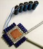
The "PCB", 40mm x 40mm is size, is an attempt to avoid making a real PCB while still having the same properties like a real square array of caps. It is made from two sheets of rather thick 200µm (8mil) copper foil spaced with a thin paper insulation of about the same thickness. This offers very low impedance paths for the rows of capacitors soldered along the edges, 22pcs. total, each 33uF/63V, being only moderate ESR but low ESL types (which is crucial). They were choosen because they were at hand and had the favorable, low inductance 2.5mm lead spacing.
Then some bigger caps (5x 2200µF/50V) are attached to that with a short piece of cabling selected in resistance to match the total ESR of the array (which was arbitrary decision for "good looks", at lower audio freqs one might whish to reduce supply impedance as much as possible. Total capacitance is about 11,000µF.
On the analyser, impedance looks like this :
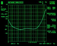
Note while not being super low in absolute terms with a baseline of about 20..30 miliohms, the nice thing is that this impedance stays flat up to 5MHz, the region of interest of typical (chip-type) power amplifiers. No resonances coming from paralleling the "wrong" film caps are seen, only an inductive rise above the bandwidth where it cannot cause harm. Residual inductance looks to be less than 1nH.
The supply characteristic of this composite capacitor should be excellent, high-frequency currents (from the half-wave rectification of load currents when class-B is entered) cannot exite any disturbing resonances.
To me, this kind of arrangement (paralled 'lytics, no film types) looks like being a very good local decoupling scheme for chipamps. By doubling up everything impedance graph can be shifted down another 6dB (0.5x) per doubling whenever levels below 10mR should be needed at RF frequencies (>100kHz)

The "PCB", 40mm x 40mm is size, is an attempt to avoid making a real PCB while still having the same properties like a real square array of caps. It is made from two sheets of rather thick 200µm (8mil) copper foil spaced with a thin paper insulation of about the same thickness. This offers very low impedance paths for the rows of capacitors soldered along the edges, 22pcs. total, each 33uF/63V, being only moderate ESR but low ESL types (which is crucial). They were choosen because they were at hand and had the favorable, low inductance 2.5mm lead spacing.
Then some bigger caps (5x 2200µF/50V) are attached to that with a short piece of cabling selected in resistance to match the total ESR of the array (which was arbitrary decision for "good looks", at lower audio freqs one might whish to reduce supply impedance as much as possible. Total capacitance is about 11,000µF.
On the analyser, impedance looks like this :

Note while not being super low in absolute terms with a baseline of about 20..30 miliohms, the nice thing is that this impedance stays flat up to 5MHz, the region of interest of typical (chip-type) power amplifiers. No resonances coming from paralleling the "wrong" film caps are seen, only an inductive rise above the bandwidth where it cannot cause harm. Residual inductance looks to be less than 1nH.
The supply characteristic of this composite capacitor should be excellent, high-frequency currents (from the half-wave rectification of load currents when class-B is entered) cannot exite any disturbing resonances.
To me, this kind of arrangement (paralled 'lytics, no film types) looks like being a very good local decoupling scheme for chipamps. By doubling up everything impedance graph can be shifted down another 6dB (0.5x) per doubling whenever levels below 10mR should be needed at RF frequencies (>100kHz)
Very nice, Klaus.
A 2-sided PCB for that would not require any etching. You would just need to drill the holes for one of each of the capacitor leads and then use a larger bit of some sort, in your drill, to remove a small ring of copper from around the edge of the hole for each cap, so one lead could go to the bottom side of the board without being able to contact the top-side copper. The leads on the top side would just be bent flat against the copper (after cutting to a reasonable length), and soldered. Just cut the leads on the bottom side to one cm or so, bend over to be flat against the copper, and solder.
A 2-sided PCB for that would not require any etching. You would just need to drill the holes for one of each of the capacitor leads and then use a larger bit of some sort, in your drill, to remove a small ring of copper from around the edge of the hole for each cap, so one lead could go to the bottom side of the board without being able to contact the top-side copper. The leads on the top side would just be bent flat against the copper (after cutting to a reasonable length), and soldered. Just cut the leads on the bottom side to one cm or so, bend over to be flat against the copper, and solder.
Thanks, Tom,
I'll probably use your method once the final types of small electros that I've ordered are here, then some bigger but space-efficient arrays have to be built. For this amount of paralled parts the edge-mount method becomes inefficient (it would require a stacked set of "cap sheets" paralleled again, sounds quite awkward).
For small test builds the edge mounting provides some flexibility, though... ease of desoldering the caps etc.
Today for something different and quite exiting : Inductance Cancellation of Filter Capacitors.
In an IEEE paper from 2004 [1] a technique is described how to lower the apparent ESL of a filter capacitor (three terminals; in, ground, out) by means of coupled inductances. This creates a negative inductance counteracting the capacitor intrinsic and wiring inductance, alongside with producing higher input/output inductance (not a bat thing) and more radiated magnetic and electric field energy at RF frequencies (less so).
I always wanted to try that in real life and now with the network analyzer allowing me to visualize and adjust this kind of things I did some quick&dirty test builds, based on the center-tapped inductor method following the paper guidelines and some SPICEing.
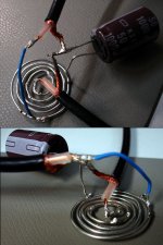
First I tried a spiral coil together with a 1000uF/50V electrolytic, after a some time of tweaking the input and ouput attach points it looked like this :
Three-terminal transfer function (@75R I/Os) plot of cap alone vs. full network :
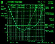
Scaling is choosen to coincide with the two-terminal impedance measurements and reading dB ref 1 Ohm. Note : above 20Mhz or so plots look suspicious/unreliable from both the lousy build (in RF terms) as well as the analyser not being normalized (normalization turned out to be problematic when the full 6 decade frequency span is used in log freq mode with the analyser on the edge of it's capabilites).
The low/flat region extends one decade higher which I found quite remarkable. At the cursor position (6Mhz) the difference in attenuation is 22dB, more than 10x. I suspect the higher ESR comes from the weak solder joint at one of the cable shields.
The effect is *extremely* sensitive to tiny geometry changes and nearby metal parts etc. Misadjusted it easily just gets worse than the plain cap. That is the weak point of any cancellation methods.
Next try, a 4700/63 bigger can (30mm dia.) with a tubular coil. The tubular coil turned out to be much easier to adjust than the spiral one in both total inductance, balancing (50:50) and mutual coupling.
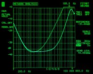
With a little trick I could arrive at the follwing plot :
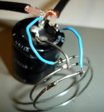
The trick was to insert a small steel core (pliers, ie) which made the flat section really horizontal. With air core, there was a slightly upwards slope from 100kHz to 5Mhz like in the previous plot. Unclear about the exact mechanism behind it (eddy currents / skin effects helping here?) and whether the improvement would hold in an actual supply filter circuit with high power signals and DC current present.
Anyway, again at 10x improvement at RF in filter attenuation is seen, not bad for two turns of copper wire in such a simple experimental setup. This thing really seems to work when implemented properly (note that at least part of it might be patented in the US by the inventors and the MIT, last time I checked I found notes indicating this).
[1] Filters and Components With Inductance Cancellation,
Timothy C. Neugebauer, Student Member, IEEE, Joshua W. Phinney, Student Member, IEEE, and
David J. Perreault, Member, IEEE,
IEEE TRANSACTIONS ON INDUSTRY APPLICATIONS, VOL. 40, NO. 2, MARCH/APRIL 2004, Pg. 483ff.
In an IEEE paper from 2004 [1] a technique is described how to lower the apparent ESL of a filter capacitor (three terminals; in, ground, out) by means of coupled inductances. This creates a negative inductance counteracting the capacitor intrinsic and wiring inductance, alongside with producing higher input/output inductance (not a bat thing) and more radiated magnetic and electric field energy at RF frequencies (less so).
I always wanted to try that in real life and now with the network analyzer allowing me to visualize and adjust this kind of things I did some quick&dirty test builds, based on the center-tapped inductor method following the paper guidelines and some SPICEing.
First I tried a spiral coil together with a 1000uF/50V electrolytic, after a some time of tweaking the input and ouput attach points it looked like this :

Three-terminal transfer function (@75R I/Os) plot of cap alone vs. full network :

Scaling is choosen to coincide with the two-terminal impedance measurements and reading dB ref 1 Ohm. Note : above 20Mhz or so plots look suspicious/unreliable from both the lousy build (in RF terms) as well as the analyser not being normalized (normalization turned out to be problematic when the full 6 decade frequency span is used in log freq mode with the analyser on the edge of it's capabilites).
The low/flat region extends one decade higher which I found quite remarkable. At the cursor position (6Mhz) the difference in attenuation is 22dB, more than 10x. I suspect the higher ESR comes from the weak solder joint at one of the cable shields.
The effect is *extremely* sensitive to tiny geometry changes and nearby metal parts etc. Misadjusted it easily just gets worse than the plain cap. That is the weak point of any cancellation methods.
Next try, a 4700/63 bigger can (30mm dia.) with a tubular coil. The tubular coil turned out to be much easier to adjust than the spiral one in both total inductance, balancing (50:50) and mutual coupling.

With a little trick I could arrive at the follwing plot :

The trick was to insert a small steel core (pliers, ie) which made the flat section really horizontal. With air core, there was a slightly upwards slope from 100kHz to 5Mhz like in the previous plot. Unclear about the exact mechanism behind it (eddy currents / skin effects helping here?) and whether the improvement would hold in an actual supply filter circuit with high power signals and DC current present.
Anyway, again at 10x improvement at RF in filter attenuation is seen, not bad for two turns of copper wire in such a simple experimental setup. This thing really seems to work when implemented properly (note that at least part of it might be patented in the US by the inventors and the MIT, last time I checked I found notes indicating this).
[1] Filters and Components With Inductance Cancellation,
Timothy C. Neugebauer, Student Member, IEEE, Joshua W. Phinney, Student Member, IEEE, and
David J. Perreault, Member, IEEE,
IEEE TRANSACTIONS ON INDUSTRY APPLICATIONS, VOL. 40, NO. 2, MARCH/APRIL 2004, Pg. 483ff.
Last edited:
Looks like you are getting some value out of the network analyser.
Though it probably will not have any effect at these frequencies, feeding the capacitor array from the centre will have a lower impedance than feeding it from the edge.
I use double sided board for this type of work and drill the holes, you can buy little copper rivets to make via's which are used on one capacitor lead to pass it through to the top side of the circuit board. No etching required.
Using such a technique it is easy to pepper a circuit board with capacitors. Large capacitor banks for industrial SMPS's are done the same way except the vias are not needed because the screw terminal post makes contact with the top side.
That centre tapped inductor idea is neat.
The low impedance needs to be seen by the load, not the feed point. How would feeding at the center of the cap array benefit the load? And where would the load be attached?
Also, why would vias be needed? Terry Given just drilled a single hole for each cap, and removed the copper from the rim of the hole (with a Dremel-type tool, with some larger bit), on the component side, so one lead from each cap could go to the other side without shorting to the component-side copper. I guess I don't understand how you are using the vias. Isn't one side power and the other side ground?
Also, why would vias be needed? Terry Given just drilled a single hole for each cap, and removed the copper from the rim of the hole (with a Dremel-type tool, with some larger bit), on the component side, so one lead from each cap could go to the other side without shorting to the component-side copper. I guess I don't understand how you are using the vias. Isn't one side power and the other side ground?
I thought this was a measurement of the properties of a capacitor array. The load is another matter, for low impedance work the load and the capacitors are in very close proximity on the same ground and supply planes,The low impedance needs to be seen by the load, not the feed point. How would feeding at the center of the cap array benefit the load? And where would the load be attached?
How would you solder to the top supply plane? If using RB/BL capacitors there is no access for the soldering iron between the top plane and the capacitor lead. So you drill the holes and install the rivets which are soldered to the top plane only, clearance is cut on the bottom plane so that the rivets do not become vias Then the capacitor leads are inserted, one goes though the pcb and is soldered to the bottom plane the other goes though the hollow rivet and is soldered to it forming the connection to the top planeAlso, why would vias be needed?
The example that was discussed in another thread used one hole per capacitor, with the copper removed from a small ring around each hole edge, for one lead to go to the bottom of the board. The other lead was bent to lay flat against the top copper, trimmed so that about a centimeter protruded out from under the cap, and soldered to the top copper.
The set of links to all of the posts about that example capacitor array are at the bottom of the post at http://www.diyaudio.com/forums/chip-amps/224914-lm3886-component-selection-3.html#post3282640 .
The set of links to all of the posts about that example capacitor array are at the bottom of the post at http://www.diyaudio.com/forums/chip-amps/224914-lm3886-component-selection-3.html#post3282640 .
- Status
- This old topic is closed. If you want to reopen this topic, contact a moderator using the "Report Post" button.
- Home
- Amplifiers
- Power Supplies
- Network Analyser Measurements