Yeah, fast or slow couldn't refer to the speed of the electricity itself, but, rather, probably to the speed with which the signal amplitude can change, at the output. And that can vary fairly widely. Or it might refer to the frequency response's upper limit, which would be related to the former.
Yeah, fast or slow couldn't refer to the speed of the electricity itself, but, rather, probably to the speed with which the signal amplitude can change, at the output. And that can vary fairly widely. Or it might refer to the frequency response's upper limit, which would be related to the former.
Tom, based on this fact, and the one that many people recommend adding large value (1uF-1000uF) bypass capacitors right at the power pins of the amplifier boards or if possible at the very side of the output devices is that I can't clear out some big doubts.
Some people say that if you install a fare amount of bypass capacitance as close as possible to the output devices, transients will be better handled as the requiered power for the transient will be delivered FIRST by the bypass capacitors until the large filter ones start to deliver their own charge. This is mostly the reason why bypass capacitors are adviced to be installed.
Well, I must admit this sounds WAY nonsense to me
 . Even without having made any specific test to support my thinking.
Some people also say -AFAIU- that they hook up the bypass capacitors through low value resistors (0.15 ohm or so). I can't get why someone would want to manually increase the ESR value
My understanding is that being both the large filter capacitors and the bypass ones at the power pins interconnected through heavy gauge wires, this provide a very low resistive path between them.
Then, how in this world would the bypass capacitors give out their charge FIRST being tied up to such big tanks like the filter capacitors are??
Voltage charge works in this case, and in many others as well, as liquid fluids.
I would agree with this to be true if there was a high resistive path between both -main bank and bypass-, in which case, once the bypass capacitors had delivered their charge they wouldn't be able to recharge any faster than that resistive path allows.
I would also agree the theory might be true if there was a fair amount of inductance in the line between the main filter bank and the bypass bank, and that to be true only at a certain frequency range close to resonant, which might also be outside the audible range of the PA frequency response.
Having said all of this, I'm close to being certain that high value bypass capacitance is, in any case, not fulfilling the planned task . Of course I might be missing something important and maybe all I said is wrong so please, anybody and everybody, feel free to point out any error or missing fact.
One big question would be, if PSU is a decent one - even not an outstanding one, just a good average PS with sufficient power for the task, wouldn't the audio quality be just dependent on the PA design? and of course of the passive crossovers and loudspeakers?
It's been recorded pages back on this thread that great sounding amplifiers with LOTS of deep bass have what looks like powerfull (BIG transformer) but of mediocre design PSU.
I repeat, I'm no EE.
A simple way of looking at it, is that the design of the PA is usually based on the concept that the voltage rails are "perfect". Spice simulations, back of envelope guesstimates, start with ideal DC voltages being "just there". Well, when you do real simulations, and real measurements, they tell you something totally different, the power supplies are varying inputs to the PA circuit in their own right.
Once you dispense with the concept that the power supply is one black box, and the PA circuit is another, that just happen to occupy a particular casing, then everything changes. The amplifier is one circuit, that happens for convenience of thinking to be separated into 2 sub-parts. The electrons don't know which sub-part they're in, they just behave as the electrical forces influencing them dictate they should ...
Frank
Last edited:
Tom has differentiated (correctly IMO) bypass and decouple within this thread. A 1μF bypass cap should shunt transients around the device, while a 1000μF decoupling cap should provide energy storage right where it's needed, to prevent affecting the entire DC supply....many people recommend adding large value (1uF-1000uF) bypass capacitors right at the power pins of the amplifier boards or if possible at the very side of the output devices...
Inductance not just in the line between the main filter bank and the bypass bank, but within the banks, too. Which puts an inductance in parallel with a capacitance. The "ESR boost" can squash the resonance, at least at critical frequencies.Some people also say -AFAIU- that they hook up the bypass capacitors through low value resistors (0.15 ohm or so). I can't get why someone would want to manually increase the ESR value...<snip>...I would also agree the theory might be true if there was a fair amount of inductance in the line between the main filter bank and the bypass bank, and that to be true only at a certain frequency range close to resonant, which might also be outside the audible range of the PA frequency response.
you said "high resistance", where you should have used "high impedance"..........................................I would agree with this to be true if there was a high resistive path between both -main bank and bypass-,.................................................
I would also agree the theory might be true if there was a fair amount of inductance in the line between the main filter bank and the bypass bank, ........................
Then everything falls into place.
Sex,
Maybe it will become clear if you first imagine a chipamp power pin with NO local capacitance:
For a given conductor size and shape, inductance increases with length. So the farther away the PSU is, the longer it would take for a needed fast-changing current amplitude to arrive (and the larger the rail-voltage dip would be). So without ANY decoupling or bypass caps at the chipamp, the speed of the transient response, and the upper limit of the overall frequency response, will depend on the distance to the PSU.
Also, you will just have to accept the fact that the response speed of a local cap will not be lowered by having a large capacitance at the PSU.
Also, keep in mind that we need the frequency response and the speed of the transient response to be WAY higher than the audible range, because the amplifier will always be trying to cancel high-frequency harmonics.
It should be clear, now, that SOME amount of decoupling capacitance is beneficial. So now it's just a matter of figuring out how much, based on the needed or desired upper end value of the frequency response.
The benefits of adding even more C than is actually required, right at the amp, will usually quickly diminish, since the rails' and capacitors' inductance will cause less of a problem for lower frequencies. But more C close to the amp would never hurt anything.
Last edited:
Sorry, I understated the benefits of using as much decoupling capacitance as possible, right at each output device, and actually omitted their main purpose:
While the high-frequency response can impose requirements for a minimum value and a maximum connection length from the point of load, for the decoupling capacitance, and while avoiding high-frequency and transient response distortions might not provide a compelling reason to increase the decoupling capacitance value by too much, past a certain point, I forgot to mention, in my last post, that "decoupling" alone is a very good reason to increase the decoupling capacitance. The main benefit of more local decoupling capacitance is lower-amplitude disturbances of the voltages rails, everywhere else in the system.
I think that in most cases, for audio power amplifiers at least, there will need to be three sets of capacitors near each output device:
1. Bypass - a small cap right across power/gnd pins, to prevent instability
2. Decoupling for transient and HF responses - inductance/connection-length is a concern; might often be under 500 uF
3. Decoupling in general - board-level or sub-system-level or device level; typically has at least as much capacitance as is needed in order to meet ripple-voltage spec for worst-case sustained low-frequency (or DC) output signal.
Thanks sofaspud and AndrewT for the clarifications
Tom, special thanks to you for taking your time to elaborate an explanation about decoupling capacitance I feel this topic makes far more sense to me now, and feel I learned something important.
I'm at a fast pace with a PA project using this boards:
LME49830 K1530 J201 300W Mono Power Amplfier Board | eBay
I also already have both channels massive toroids and many other parts. When ready to start I'll open a thread in the correct forum section.
Still need a nice enclosure; and price rises exponentially with beauty like in many areas of life..
Tom, special thanks to you for taking your time to elaborate an explanation about decoupling capacitance
I feel this topic makes far more sense to me now, and feel I learned something important.I'm at a fast pace with a PA project using this boards:
LME49830 K1530 J201 300W Mono Power Amplfier Board | eBay
I also already have both channels massive toroids and many other parts. When ready to start I'll open a thread in the correct forum section.
Still need a nice enclosure; and price rises exponentially with beauty like in many areas of life..
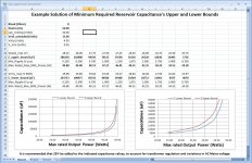
I think I just did something that could be useful and maybe even interesting. It's about calculating reservoir capacitances.
See: http://www.diyaudio.com/forums/chip-amps/230787-lm3875-gainclone-too-much-treble-3.html#post3403933
Attached is an image of a spreadsheet that I threw together, to turn the crank on the equations, for me.
It has a plot of the upper and lower bounds of the minimum required reservoir capacitance vs the Max Rated Output Power (to just barely avoid clipping).
given the unloaded rail voltage, the Vclip voltage (across the amp), which is given in the LM3875 datasheet in this case, and Rload, fmains, and an increment to change the resulting Vpeak_max voltage by, and maybe some other things; just take a look.
Basically, I was able to express everything (e.g. peak current and max ripple voltage) in terms of one unknown variable, such as the max peak output voltage, plus a few variables that become fixed parameters for any particular case.
I was actually able to eliminate the need to manually select or calculate or guess at the acceptable ripple voltage amplitude. It's just calculated in terms of Vrail_unloaded, Vclip, and Vpeak_max (output peak voltage), the first two of which are assumed to be known.
However, you can still select the capacitance value based on the p-p ripple, or based on the Vpeak_max output voltage, or based on the Max Rated Output Power. Those are all dependent on only one of the others. i.e. Know one and you know them all. So I just sweep the Vpeak_max and calculate the minimum required C for each step, and then also calc the equivalent ripple amplitude and Max Rated Output Power.
And the fixed parameters in the upper left corner can just be changed at will, and everything automatically recalculates.
I DO HOPE that someone will check the derivation for accuracy, at the link given above! Then maybe I can post a similar spreadsheet.
Cheers,
Tom
Attachments
Last edited:
No.
The sensible maximum when the open circuit rail voltage is @ +-33Vdc is about 45W.
A more practical maximum would be around 40W from +-33Vdc supply rails.
We are back to the same old idea of asking a too low voltage transformer to deliver impossibly high claimed power figures.
If you want 50W then use a higher rail voltage.
If you want 60W then the next step up in rail voltage is warranted.
The spreadsheet would make the number crunching very easy.
that's a lot!
Alas, you do not see how much difference 1.5V can make.
Read the graphs !!!!
40W is modeled as needing between 14.5mF and 20mF, not 288mF
You're right. But anyway I was not expecting to see such high values when the power is just a little more.
Keep in mind that the resulting capacitances are not what is needed "to sound good". They are the absolute minimum capacitance needed to prevent any clipping at all, when the amp is producing its MAXIMUM rated output power. Actually, they determine the max rated output power.
Why are some of them so large? Basically, I just selected some of the Vpeak_max values to show the impractical cases, just to illustrate the concepts.
As the Vpeak_max is pushed up, to get a higher max rated output power, there is less voltage space for the ripple to occupy. The maximum rail voltage is what it is, and the amplifier's Vclip figure (between +rail pin and output pin) can't occupy less than 4.5V (when the rail is 33V, according to datasheet) of the voltage space between the signal maximum and the ripple minimum. When you try to increase Vpeak_max too much and start to run out of room in the voltage space, the ripple amplitude needs to get stupidly small in order to fit, and not cause clipping, so the capacitance gets stupidly large. You would probably never want to try to cut it that close, anyway.
Note, too, that the upper-bound C value is calculated based on an absolutely-worst-case output current, i.e. the current is DC, but at the maximum sine peak current that the amplifier should be capable of producing. So it's 1.414 times higher than the maximum RMS current that the amp should be expected to produce.
I originally settled on that type of DC output (i.e. at the maximum peak sine level) as being the worst case, way back when I was worried about different phase relationships between the charging pulses and the sine signal, since the DC would cover all of those. But in thinking about lower and lower sine signal frequencies, much lower than the charging pulses' repetition rate, with the worst case (integral of the current waveform) being when the sine's peak was centered between charging pulses, it became obvious that as the sine signal frequency went toward zero and its peak grew very wide, its waveform, with peak centered between charging pulses, would approach DC at the sine's peak level.
At any rate, it seems intuitively clear that the upper-bound capacitance that is derived in that way will always be able to supply the current needed, for any signal waveform with a voltage amplitude that never exceeds Vpeak_max.
BUT, in real music, e.g. live music, with more than one tone or instrument waveform present at the same time, there could often be coincident peaks, where the amplitudes would sum. This analysis had to assume that no voltage peaks exist, in the input waveform, would cause the output to need to be greater than Vpeak_max volts.
Last edited:
- Status
- This old topic is closed. If you want to reopen this topic, contact a moderator using the "Report Post" button.
- Home
- Amplifiers
- Power Supplies
- Power Supply Resevoir Size