Steven,
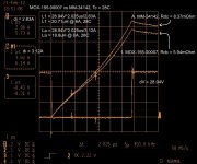
this is not an audio amplifier - its a "splat tester" for measuring inductance, but I used the aforementioned construction technique.
The Splat Tester is a big bank of caps going to a coil under test, then into a FET switch to 0V (many FETs in parallel). On the other side of the PCB is +Vdc, and a slot cut across the PCb. I solder the choke I'm testing across the slot.
There is a loop of wire I clip my current probe onto, and a pulse generator drives the input of a FET driver. The diodes you see are between the FET Drains and +Vdc.
I feed the cap bank from a bench supply, up to 100V. Then whack the choke with a pulse from a pulse generator. This makes current build up in the Choke being tested:
V = L*dI/dt, so for t = Tpulse, I ramps up to Vdc*Tpulse/L_choke
the slope of the measured current dI/dt = Vdc/L_choke, so I can calculate
L_choke = Vdc*Tpulse/I
I ensure that 0.5*6.5mF*Vdc^2 is >> 0.5*L_choke*I^2 (or in other words that +Vdc doesnt droop much)
there is a BNC connector for the pulse generator input, another to connect a scope probe to the input pulse (to trigger from) and a BNC measuring Vdrain.
This way I can measure inductance vs current, and see saturation too. with ferrite cores the current slope is straight, until it saturates (which is quite sharp). iron powder cores have a permeability that varies a lot with current, so the current slope isnt straight, nor is the transition into saturation very pronounced.
attached are splat test results from Iron Powder (Moxie...) and Ferrite (NGD....) cored inductors.
Only downside to this toy is I used a plastic box. So I had to cobble together a heat shield from FR4, so I can het the device under test to 100C without melting the box, or my horribly expensive current probe")
You can make a crude version of this with a decent sized cap bank, and a low inductance current sensing resistor. stick the R in series with the cap -ve terminal, and hook a scope probe to it. stick another scope probe to the + terminal. solder one leg of the DUT onto one cap terminal, and use a bit of solid wire soldered to the other terminal as a switch. charge the caps up, then close the switch - you'll soon see why its called a SPLAT test! eventually you will get sick of poor contacts (bounce = lousy waveform) and make a box like this.
I learned this trick years ago, working on big AC drives. 40mF charged to 600Vdc makes quite an impressive splat, and is a great way of getting several hundred amps flowing into a choke. ever so slightly lethal though......
this is not an audio amplifier - its a "splat tester" for measuring inductance, but I used the aforementioned construction technique.
The Splat Tester is a big bank of caps going to a coil under test, then into a FET switch to 0V (many FETs in parallel). On the other side of the PCB is +Vdc, and a slot cut across the PCb. I solder the choke I'm testing across the slot.
There is a loop of wire I clip my current probe onto, and a pulse generator drives the input of a FET driver. The diodes you see are between the FET Drains and +Vdc.
I feed the cap bank from a bench supply, up to 100V. Then whack the choke with a pulse from a pulse generator. This makes current build up in the Choke being tested:
V = L*dI/dt, so for t = Tpulse, I ramps up to Vdc*Tpulse/L_choke
the slope of the measured current dI/dt = Vdc/L_choke, so I can calculate
L_choke = Vdc*Tpulse/I
I ensure that 0.5*6.5mF*Vdc^2 is >> 0.5*L_choke*I^2 (or in other words that +Vdc doesnt droop much)
there is a BNC connector for the pulse generator input, another to connect a scope probe to the input pulse (to trigger from) and a BNC measuring Vdrain.
This way I can measure inductance vs current, and see saturation too. with ferrite cores the current slope is straight, until it saturates (which is quite sharp). iron powder cores have a permeability that varies a lot with current, so the current slope isnt straight, nor is the transition into saturation very pronounced.
attached are splat test results from Iron Powder (Moxie...) and Ferrite (NGD....) cored inductors.
Only downside to this toy is I used a plastic box. So I had to cobble together a heat shield from FR4, so I can het the device under test to 100C without melting the box, or my horribly expensive current probe
You can make a crude version of this with a decent sized cap bank, and a low inductance current sensing resistor. stick the R in series with the cap -ve terminal, and hook a scope probe to it. stick another scope probe to the + terminal. solder one leg of the DUT onto one cap terminal, and use a bit of solid wire soldered to the other terminal as a switch. charge the caps up, then close the switch - you'll soon see why its called a SPLAT test! eventually you will get sick of poor contacts (bounce = lousy waveform) and make a box like this.
I learned this trick years ago, working on big AC drives. 40mF charged to 600Vdc makes quite an impressive splat, and is a great way of getting several hundred amps flowing into a choke. ever so slightly lethal though......
Attachments
Steven,
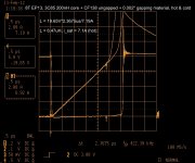
here is the impedance of the cap bank. vertical scale in dB-Ohms, top line = 40dBOhms.
I also measured an SMH 25V 12,000uF = 12mF capacitor. I dont have a dedicated test fixture for this cap, so the measured lead inductance is a bit higher than ESL (I had to have enough leads to solder the darned thing to an existing test fixture). I'd estimate this cap at around 7-10nH (test fixtures are important when measuring stupidly low inductance).
But the cap bank has a total of 1.7nH - almost 10x better. and there are NO nasty resonances out to 200MHz (HP3577A limit). Nor are there any "decoupling" caps (film or otherwise)! yet the Dc bus impedance is < 100mOhms @ 2MHz, rising to 1 Ohm at 90MHz.
Not bad for a home-made PCB, using only a battery drill
The cap bank is very crude - a DS-PTH pcb would shave off maybe 0.2~0.5nH. Using thinner PCB (this is 1.6mm) would have a much larger effect - I would expect a total inductance of < 0.5nH in that case.
Edit: this very low broadband impedance will do a VERY good job of attenuating any AC line noise that makes it past the rectifiers. Likewise this will effectively filter any audio signal above 1kHz or so, preventing it from reaching the transformer. assuming, of course, one does not then go and undo all this good work with lousy wiring.
I genuinely do not understand why the DC bus layout of audio amps is so horrendously bad. it need not be, and the cost is almost zero.
cheers
Terry
Attachments
Last edited:
I've noticed something on the Honey Badger.
It has 470u//220u aboard.
This will give you a wonderfully balanced tone.
For personal preference, I would add 1 of 2u 250v cap (polyester, electro, or RC) v+ to v- for noise block (takes some experimentation to find the right cap for desired clean cool laid back effect of noise blocking), but that is not in question.
Here's some question:
The 220u is greatly responsible for the clarity and tone of the amp (as always, the smallest electro on an amp board governs the tone), and I think an excellent choice. The 470u is not greatly responsible for the clarity and tone of the amp--they are defense. Could I not replace the 470u with 3300u? Perhaps if I combined a high efficiency 220u with a standard 3300u, the ESR would come closer to matching and one cap wouldn't fight the other for charge. For clarity and tone, it is necessary that the 220u Always Wins the fight for charge.
Ideas?
Other way to say it: The Honey Badger board, and the LM1875 chip alike, lump together the predrive bypass caps (220u) and the output bypass (470u) into one paralleled section. This is inconvenient and a bit confusing, both to myself and to the capacitors when they compete for charge. The simplistically paralleled grouping is the only option for the LM1875 chip due to limited number of power input pins. However, the Honey Badger is a discrete amp with no such limitation. I'd like to know how to use the 220u for predrive and locate the 470u (or larger) more effectively to accomplish their individual tasks. I'd like to assure that the 220u predrive caps aren't needlessly drained when a bass beat is delivered by the outputs. The layout contains no such guarantee, and the loop area is very, very big.
Last edited:
The 470uF and 220uF are not in parallel, as there is a 22ohm resistor between them according to the circuit diagram. When capacitors compete for the available charge they never get confused but always follow the laws of electromagnetism and Ohm's Law etc.
470uF appears to be an on-board local decoupler for the output, and the 220uF does a similar job (plus a small amount of smoothing) for the driver. Presumably the 470uF is in parallel with the main PSU caps. Increasing its value would have the main effect of bringing more charging pulse current onto the amp PCB - perhaps a bad idea?
470uF appears to be an on-board local decoupler for the output, and the 220uF does a similar job (plus a small amount of smoothing) for the driver. Presumably the 470uF is in parallel with the main PSU caps. Increasing its value would have the main effect of bringing more charging pulse current onto the amp PCB - perhaps a bad idea?
The size of the "pulse" current will be limited by the emf driving that pulse and the impedance trying to resist that pulse.
The cables are very effective pulse limiters.
Look at Peter Daniel's implementations where he completely foregoes all PSU smoothing and uses local decoupling of 1mF to 1m5F on the amp PCB. He says great for mid and highs (yes the MF and HF decoupling is doing it's job).
The cables are very effective pulse limiters.
Look at Peter Daniel's implementations where he completely foregoes all PSU smoothing and uses local decoupling of 1mF to 1m5F on the amp PCB. He says great for mid and highs (yes the MF and HF decoupling is doing it's job).
A commercial amplifier design I did a few years back had a pair of 3m3F + 33µF all on the same board with the amplifier (50W x2), everyone was stunned at how much better it sounded than the run-of-the-mill commercial amplifiers (Adcom, etc.). A 160VA transformer was used.
Hi again,
Progress update: i have been running simulations with the new per-unitized transformer model, which is able to be scaled to different Volt-Amp ratings and different Output Voltage ratings simply by changing the values of two corresponding spice parameters. (Thank you, Terry Givens!!)
I have found at least two interesting and suprising patterns while finding the minimum reservoir capacitance that doesn't allow the transformer current pulses to cause the rail voltage to make overt incursions into the output signal voltage. These were found after I refined the methods used so that the output amplitude and offset were initially set very precisely and then the calculated output expression was precisely matched to that, so that the calculated difference between them gave much more accurate error and distortion measurements.
Also, because of the easy-to-use scalability of the VA and Vrms ratings of the new xfrmr model, i was able to try, for example, large VA xfrmrs with high-enough Vrms ratings for cases with relatively-low output power specs, and was able to simulate broader ranges of output power values for a given transformer size.
I have only begun to scratch the surface, because my available "play time" has been severely limited, lately. So i have more to do before I can hope to have any comprehensive or definitive results to share. I mainly wanted to let Nico know that the work is still progressing.
But, so far, it looks like whenever the VA and the Vrms ratings are "large enough" then the absolute-minimum reservoir capacitance is much lower than I would have guessed. This is not really surprising, maybe. But I was surprised by the consistency of the numbers, between cases with widely-varying transformer ratings and output power specs. For example, with a 44 Vrms xfrmr output rating and various appropriate VA and signal output power specs, the minimum C values were all in a narrow range, under 500 uF.
The other thing I noticed is probably also not as surprising as I thought: i can predict (or find) the minimum C value by looking at the minimum difference between the maximum signal output peak voltage and the minimum power rail voltage. For the 44 vct case, with VA all the way from 1000 to 240 and output power of 100 Watts, 75W, 50W, and even 25w (all different peak output voltages), that difference doesn't change, staying at about 3.35 volts, but going down to just above 3.0 volts for some of the 25W output cases.
When I simulate a series of C-value steps for a new configuration of VA, Vrms, and Pout, I usually first look at the tabulated measured vrailmin minus vsignalmax that I now have spice find for me. I can _always_ select the two C value steps where the last few hundred uV of the overt charging pulse distortion finally disappears, that way.
In the meantime, i am also collecting all of the data to eable plotting the distortione versus C value for each case.
When I get some more time i will probably first see how the results i have so far correspond to what would be predicted using a constant DC load, since I am finally at a point where the measurements are staying consistent.
More later,
Tom
Last edited:
True. It is exactly what I would expect. With a big enough off-load rail voltage you can have lots of droop/ripple without causing problems. Hence my belief that there is no absolute minimum capacitance.gootee said:But, so far, it looks like whenever the VA and the Vrms ratings are "large enough" then the absolute-minimum reservoir capacitance is much lower than I would have guessed. This is not really surprising, maybe.
So my wild guess of 2V was not too far out. It explains why the cap values I calculated were a bit different from the ones you found from simulation.gootee said:staying at about 3.35 volts,
Tom, thats great work! Its been my pleasure to help, and I'm learning a lot.
I'm tickled pink you've sussed out the PU xfmr model. its a really, really powerful technique, and like all good tricks, has been around a long time. back before easily accessible computing, engineers had to think really, really hard. Oh the nomograms they created - Phillip Smith was just one of many brilliant engineers.
another way to use the PU model is to ascertain bounds (eg derived from measurements over a range of xfmrs) on the PU resistances & leakage inductances. For example with mains transformers (too lazy to research so going from memory), leakage ranges from about 5% (high efficiency devices) to around 10%, with 15% being an upper bound**
it'll be different for physically smaller devices though, due to the Surface Area to Volume ratio - e.g. efficiency of small induction machines is pretty bad, because they can get rid of the heat. again from memory, with < 1kW induction motors its common to find locked-rotor currents (in PU I_locked_rotor = 1/L_leakage) of about 500%, so around 20% leakage. thats a problem from a power loss perspective (plenty of industrial plants have hundreds of small motors & drives), and the newer high-efficiency machines are more like 5%. Which of course means the locked-rotor current are now more like 2000%, creating a whole new set of problems.
I have no idea what xfmrs most people actually use, but it would be nice to assemble a repository of xfmr models. its straightforward to hack up a spreadsheet implementing your xfmr measurement protocol, and then Per-Unitising the results. the real trick is getting the xfmrs to measure. Anybody know a friendly supplier that'll lend out samples to have them characterised?
** I once had a chat with some engineers at ABB in New Plymouth, and they showed me a couple of 14% xfmrs shipped in from South America. I forget how many MVA, but they were about 10' x 10' x 10'. apparently it was a comms screwup, and the bosses were not happy. they offered to sell them to me for beer money.....
errata: my last name is singular, not plural. I dont mind at all, but am a raging pedant (here's a fun trick: tell a pedant to stop being so "pendantic" and watch their head explode)). its hilarious though - I usually say Given, as in "given a stupid name thats also in the dictionary" and most people still write Gibbon. Maybe I should use my Chinese name instead.....
Yes, DF. But also, we never did hope that there was one absolute minimum capacitance value. Actually, I don't think Nico even mentioned "minimum". That was just something that I thought we should try to find an equation or rule of thumb for, to try to start to find some bounds around what Nico had asked for, which was more like "Can we come up with a rule of thumb for how much capacitance should be used?".
Later today, hopefully, I will try to find out how that "separation voltage" changes for different combinations of Vrms rating, Rload, Pout, and VA rating.
It might be nice to be able to understand exactly how it arises and how we might calculate it (which might be obvious but I haven't had time to think about it except in terms of simulations, for quite some time now), but maybe it would not be very useful unless we also had an easy way (besides simulations) to know the minimum rail voltage.
I have been hoping that using the square wave test signal will almost-directly translate into easy calculation methods using assumed-constant DC peak load current. It's one of many things that should be easy and obvious to figure out but which I simply haven't gotten to, yet.
There are definitely differences between the square wave and the constant load current cases, such as modulation of the rail voltage amplitude at the difference frequency of the rectifier output and the square wave's repetition rate, and some other variations caused by the signal rises and falls. But since we are just looking for generic rules of thumb, we might be able to just add some small "safety margin" to account for those.
And I have only been talking about finding the bare minimum C. But that's probably not what C "should be used", anyway. It might come down to some minimum acceptable distortion level, in terms of the "normal" type of distortion, not the overt type where the rail voltage and the signal voltage get too close together and cause obvious protrusions to grossly deform the output waveform.
Recapping: That overt distortion is what I was using to find what I called "the absolute minimum C value". But after C is large-enough and that overt type of distortion is impossible, there is still an image of the rail voltage in the ideally-flat tops and bottoms of the square waves, that is what I referred to as the "normal" type of distortion. We can make that normal type of distortion smaller by adding more C. It appears to approach an asymptote as C gets very large. So there is apparently a C value that is large-enough, after which it doesn't improve very much if more C is added.
Anyway, the "absolute minimum" required C, in each case, where the overt distortion disappears as C increases, and the accompanying almost-constant vrailmin - vsignalmax voltage difference, appear to mark the region where the plot of the normal type of distortion versus C "turns the corner" from mostly vertical toward mostly horizontal and begins approaching the asymptote.
So I'm hoping that we can find that something closely related to the approximate DC-type capacitance and ripple equations can be used (in light of the square wave simulation data) to predict the absolute minimum C and/or the minimum vrailmin minus vsignalmax voltage, based on a given Rload, Pout, and xfrmr Vrms and VA ratings, and that we can also then find a simple rule for knowing how much C to add to that minimum, to also take us to a minimum-acceptable level of the normal type of distortion, down on the flatter part of the distortion vs C plot.
Cheers,
Tom
Hi All,
Tom: You certainly did a great job, I do not think that others have gone so far as to with the models in the simulation.
I followed (perhaps not very well) your work, I am with out a doubt, whereas the AC line is not perfectly sinusoidal, we know the reason of inductive loads, reactive, many big industrial capacity etc.
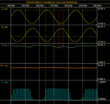
see for example, ac1-ac2 is the secondary transformer, V-in (on main capacitor cell, in relation to the load 12Amp burst 1Khz. with duration of 20mS.
there is a hole of energy is not in phase with the ac line I think.
you can show like these on your model? it is simple monitor of ac-line, main capacitor, voltage rail on power devices.
regards
Tom: You certainly did a great job, I do not think that others have gone so far as to with the models in the simulation.
I followed (perhaps not very well) your work, I am with out a doubt, whereas the AC line is not perfectly sinusoidal, we know the reason of inductive loads, reactive, many big industrial capacity etc.
see for example, ac1-ac2 is the secondary transformer, V-in (on main capacitor cell, in relation to the load 12Amp burst 1Khz. with duration of 20mS.
there is a hole of energy is not in phase with the ac line I think.
you can show like these on your model? it is simple monitor of ac-line, main capacitor, voltage rail on power devices.
regards
Attachments
My apologies, Terry! I am usually the most-pedantic person around, wherever I am. And I am always slightly startled when I realize I've made an error like that. But it seems to have helped me try to learn to be more humble and human, over the years. At this point I prefer to believe that I am just more-exhausted than usual.
Anyway, in the context of future internet searches for your name, when you're even more famous than you are now, the following might serve as a small Rosetta Stone to help mitigate my error.
I think that my error is confined to only diyaudio.com, where i have, several times, referred to Terry Given erroneously as Terry Givens.
Cheers,
Tom Gootee
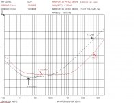
The smallest difference between rail voltage minimum and output peak maximum depends on the details of the output stage, and may vary slightly with the load resistance. In the case of your simulated output there are three Vbe drops, but also drops across the resistors - which will depend on BJT current gain. In some cases the resistors will have their value divided by the current gain, rather than setting a fixed voltage drop.
As you mention, even after gross clipping has been eliminated there may still be some 'ghost' of the ripple imprinted on the signal. That is down to the PSRR of the output stage, which it ought to be possible to estimate (even if only crudely), but it will depend on output stage architecture so no general rule of thumb will be possible. Fortunately NFB will help with this.
As you mention, even after gross clipping has been eliminated there may still be some 'ghost' of the ripple imprinted on the signal. That is down to the PSRR of the output stage, which it ought to be possible to estimate (even if only crudely), but it will depend on output stage architecture so no general rule of thumb will be possible. Fortunately NFB will help with this.
Hi again,
Progress update: i have been running simulations with the new per-unitized transformer model, which is able to be scaled to different Volt-Amp ratings and different Output Voltage ratings simply by changing the values of two corresponding spice parameters. (Thank you, Terry Givens!!)
I have found at least two interesting and suprising patterns while finding the minimum reservoir capacitance that doesn't allow the transformer current pulses to cause the rail voltage to make overt incursions into the output signal voltage. These were found after I refined the methods used so that the output amplitude and offset were initially set very precisely and then the calculated output expression was precisely matched to that, so that the calculated difference between them gave much more accurate error and distortion measurements.
Also, because of the easy-to-use scalability of the VA and Vrms ratings of the new xfrmr model, i was able to try, for example, large VA xfrmrs with high-enough Vrms ratings for cases with relatively-low output power specs, and was able to simulate broader ranges of output power values for a given transformer size.
I have only begun to scratch the surface, because my available "play time" has been severely limited, lately. So i have more to do before I can hope to have any comprehensive or definitive results to share. I mainly wanted to let Nico know that the work is still progressing.
But, so far, it looks like whenever the VA and the Vrms ratings are "large enough" then the absolute-minimum reservoir capacitance is much lower than I would have guessed. This is not really surprising, maybe. But I was surprised by the consistency of the numbers, between cases with widely-varying transformer ratings and output power specs. For example, with a 44 Vrms xfrmr output rating and various appropriate VA and signal output power specs, the minimum C values were all in a narrow range, under 500 uF.
The other thing I noticed is probably also not as surprising as I thought: i can predict (or find) the minimum C value by looking at the minimum difference between the maximum signal output peak voltage and the minimum power rail voltage. For the 44 vct case, with VA all the way from 1000 to 240 and output power of 100 Watts, 75W, 50W, and even 25w (all different peak output voltages), that difference doesn't change, staying at about 3.35 volts, but going down to just above 3.0 volts for some of the 25W output cases.
When I simulate a series of C-value steps for a new configuration of VA, Vrms, and Pout, I usually first look at the tabulated measured vrailmin minus vsignalmax that I now have spice find for me. I can _always_ select the two C value steps where the last few hundred uV of the overt charging pulse distortion finally disappears, that way.
In the meantime, i am also collecting all of the data to eable plotting the distortione versus C value for each case.
When I get some more time i will probably first see how the results i have so far correspond to what would be predicted using a constant DC load, since I am finally at a point where the measurements are staying consistent.
More later,
Tom
Hi All,
Tom: You certainly did a great job, I do not think that others have gone so far as to with the models in the simulation.
I followed (perhaps not very well) your work, I am with out a doubt, whereas the AC line is not perfectly sinusoidal, we know the reason of inductive loads, reactive, many big industrial capacity etc.
see for example, ac1-ac2 is the secondary transformer, V-in (on main capacitor cell, in relation to the load 12Amp burst 1Khz. with duration of 20mS.
there is a hole of energy is not in phase with the ac line I think.
you can show like these on your model? it is simple monitor of ac-line, main capacitor, voltage rail on power devices.
regards
AP2,
I don't understand exactly what you are suggesting but I think that I can answer your question.
In the simulation model, we can add connections and components at any point in a circuit.
One component we can add is a voltage or current source ( or a circuit including them). And they can be driven or controlled in extremely-general ways, such as by equations, or by equations involving parameters from other parts of circuits.
I am confident that we could devise a way to generate a close math to the burst you showed. And we can insert a voltage or current source into a conductor, anywhere, or connect it however we need to, in order to arithmetically sum the burst with that conductor's voltage or current.
Regards,
Tom
Thank you for reply,
certainly my English does not help me.
well, as you say, I agree, also I make models when I need it.
I suppose that you have your complete model of transformer, rectifier and main capacitors (I think you have this)
Now it is obvious that you have created a load (I hope dynamic) amplifier or as burst as you said. Now, I ask you to show the tracks in points. ac on the secondary, on main filter capacitors, and on load. as I have shown in my last post.
....where i have, several times, referred to Terry Given erroneously as Terry Givens.
Cheers,
Tom Gootee
I have on several occasions called Frank Fred, now that is a blunder of note!
Thank you for reply,
certainly my English does not help me.
well, as you say, I agree, also I make models when I need it.
I suppose that you have your complete model of transformer, rectifier and main capacitors (I think you have this)
Now it is obvious that you have created a load (I hope dynamic) amplifier or as burst as you said. Now, I ask you to show the tracks in points. ac on the secondary, on main filter capacitors, and on load. as I have shown in my last post.
AP2,
I have been running around doing unrelated tasking, so far today. So I haven't had time to study anything here on diyaudo, yet. (And my previous posts today were from my iphone.) I think that the only part that I don't understand is where and what the burst is. What causes it? Is it a current that the load is trying to draw? Or is it coming into the primary of the transformer as interference on the AC Mains? Or... what?
Tom
I have on several occasions called Frank Fred, now that is a blunder of note!
Yes, but at least there was only one time when you didn't quickly correct yourself.
- Status
- This old topic is closed. If you want to reopen this topic, contact a moderator using the "Report Post" button.
- Home
- Amplifiers
- Power Supplies
- Power Supply Resevoir Size