Performance test
I got PCBs for SuperTeddyReg and Salas Shunt, so I can build them. I don't know if K-Multiplier PCB is available, anyway I'll build it myself.
When all regulators will be ready, TWRPS included, I'll go to a professional lab to test their real performance.
All regulators will be set to 6VDC/700mA.
I got PCBs for SuperTeddyReg and Salas Shunt, so I can build them. I don't know if K-Multiplier PCB is available, anyway I'll build it myself.
When all regulators will be ready, TWRPS included, I'll go to a professional lab to test their real performance.
All regulators will be set to 6VDC/700mA.
With the exception of C1 being connected to ground, my impression has been that the K-Multiplier is supposed to be floating. I haven't simulated your circuit, but certainly my graphs (of the floating K-Multiplier) don't look like your graphs.
I will add that you can improve the floating K-Multiplier's input rejection performance at higher frequencies by splitting R2 into two resistors of 499 ohm each, and connecting another 820uF capacitor from the R2a/R2b junction to ground.
Also, the DDDac website has a 5V regulator solution that prioritizes input rejection performance and low noise, which you may find it worth looking at. The TIP122 pass device is chosen for high currents, and a smaller, less capacitive device could be chosen if lower currents are sufficient.
DDDAC 1794 NOS DAC - Non Oversampling DAC with PCM1794 - no digital filter - modular design DIY DAC for high resolution audio 192/24 192kHz 24bit
hth
I got PCBs for SuperTeddyReg and Salas Shunt, so I can build them. I don't know if K-Multiplier PCB is available, anyway I'll build it myself.
When all regulators will be ready, TWRPS included, I'll go to a professional lab to test their real performance.
All regulators will be set to 6VDC/700mA.
Subscribed!!!
Revision
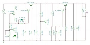
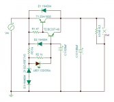
After several tests op amp series regulator has been abandoned for a total discrete components design.
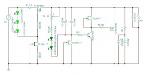
Actual schematic consists of a pre-regulation stage made by a sort of variable zener to set the voltage, followed by a capacitor multiplier. This stage acts as a pre-regulator and isolates the regulator from the load.
Follows the feedback regulation with a single bjt that drives the output devices in push-pull configuration.
For all the pass devices have been chosen the Sziklai pair mode, for its low output impedance. Also, the push-pull halves output impedance.
The values in the schematic are for a 4-9 volts 500mA regulator.
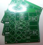
PCB can be used for both positive and negative regulator.
Also, the PCB can be used for a DC version (without rectification and filtering), cutting the PCB along the white line.
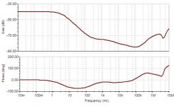
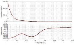
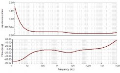
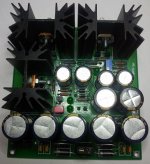
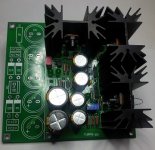
Attached: the actual schematic, some images of PCB and finished regulator, and the output impedance simulation.
After several tests op amp series regulator has been abandoned for a total discrete components design.
Actual schematic consists of a pre-regulation stage made by a sort of variable zener to set the voltage, followed by a capacitor multiplier. This stage acts as a pre-regulator and isolates the regulator from the load.
Follows the feedback regulation with a single bjt that drives the output devices in push-pull configuration.
For all the pass devices have been chosen the Sziklai pair mode, for its low output impedance. Also, the push-pull halves output impedance.
The values in the schematic are for a 4-9 volts 500mA regulator.
PCB can be used for both positive and negative regulator.
Also, the PCB can be used for a DC version (without rectification and filtering), cutting the PCB along the white line.
Attached: the actual schematic, some images of PCB and finished regulator, and the output impedance simulation.
Attachments
Ciao/Hi Andrea,
Do you sell the PCBs?
Grazie / Thanks
Felipe
Hi Felipe,
I have some extra PCB of this regulator I could sell, I have only to remember what I paid for each PCB. Let me investigate then I tell you.
If you are interested, I'm developing and SMD version of this regulator. I believe it will be ready within a month. The regulator is the same of the TH version, only rectification and filtering are omitted.
Andrea
Andrea,
could you also add the space/holes for a 'Hagerman snubber' on the ac inputs (10nF film cap in parallel with a 150nF +1/4W resistor - MKPs, or surprisingly, the polyesters MKS, work well - need the 'Quazimodo Bell Ringer' tester for the correct value of the resistor
could you also add the space/holes for a 'Hagerman snubber' on the ac inputs (10nF film cap in parallel with a 150nF +1/4W resistor - MKPs, or surprisingly, the polyesters MKS, work well - need the 'Quazimodo Bell Ringer' tester for the correct value of the resistor
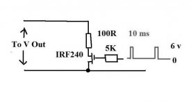
Can you load it with a pulsed current source to see how much it rings?
I don't own a pulsed current generator, but if you own one I could send you a PCB to give it a test.
BTW...
The Sziklai pair is normally happy to oscillate for some reasons you surely know, but the capacitor C13 is also happy to avoid that.
As far as I have tested the regulator:
- removing C13 without load it doesn't oscillate
- removing C13 with a resistive load (8 ohm) it oscillates
- with C13 in place without load it doesn't oscillate
- with C13 in place and resistive load (8 ohm) it doesn't oscillate
- with C13 in place and real load, Ian's FIFO board - 6V 500 mA, it doesn't oscillate
- with C13 in place and real load, Tda1541A Red Baron board - 15V around 50 mA, -5V around 50 mA, +5V around 50 mA, it doesn't oscillate
I wonder why you think that it rings.
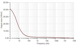
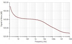
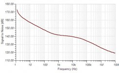
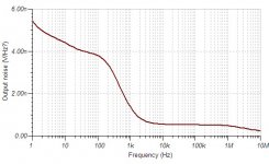
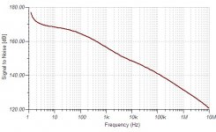
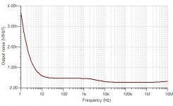
The noise is below the noise floor of my oscilloscope (1 mV resolution), but I'm building a low noise premplifier do test the noise arounf 1 uV.
andrea_mori said:I don't own a pulsed current generator, but if you own one I could send you a PCB to give it a test.
D.I.Y., example is bellow
Attachments
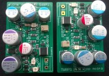
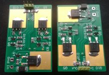
TWRPS-pp micro SMD version
For those who love SMD, this is the micro version of the TWRPS-pp, current up to around 300 mA.
Values indicated in the BOM are for 15V and 3V3 positive regulators, suitable to supply the TWCMC crystal oscillator
http://www.diyaudio.com/forums/digi...jitter-crystal-oscillator-51.html#post4241884
For those who love SMD, this is the micro version of the TWRPS-pp, current up to around 300 mA.
Values indicated in the BOM are for 15V and 3V3 positive regulators, suitable to supply the TWCMC crystal oscillator
http://www.diyaudio.com/forums/digi...jitter-crystal-oscillator-51.html#post4241884
Attachments
Andrea, do you still have pcbs for that?
Cheers
Ernst
Yes, a few TWRPS-pp micro board left.
Andrea
Very nice work!
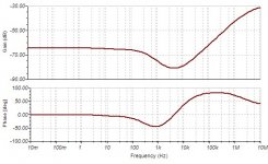
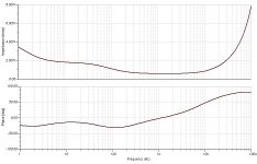
Curious to see the overshoot/ringing from the pulsed load test. The finite loopgain results in an inductive output impedance. Together with the output capacitors this often forms a resonant circuit. You could check this in the simulation too, but the output impedance is flat up to 10MHz (very good!). It could also be easily fixed with an RC circuit on the output.
I have two marks though, have you considered active rectification (with FET's and a controller) instead of schottky's with parallel capacitors?
The output impedance of those series pass transistors is generally in the shape of a diode IV curve. This would imply that the resistance is current dependant! It could lead to some ripple when output current is pulsed. You could lower it by forcing some current draw (I like LED's, because they give a nice visual indication as well") ). Shunt reg's don't have this problem because the series pass transistor of the CCS delivers, as the name suggest, a constant current.
). Shunt reg's don't have this problem because the series pass transistor of the CCS delivers, as the name suggest, a constant current.
Another suggestion would be to make a negative variant of the 12V. Many headphone/pre/phono amplifier fanatics would be happy so. Though I can understand you've got your hands full with the TWTMC, Reclocker and now the TWRPS as well.
Curious to see the overshoot/ringing from the pulsed load test. The finite loopgain results in an inductive output impedance. Together with the output capacitors this often forms a resonant circuit. You could check this in the simulation too, but the output impedance is flat up to 10MHz (very good!). It could also be easily fixed with an RC circuit on the output.
I have two marks though, have you considered active rectification (with FET's and a controller) instead of schottky's with parallel capacitors?
The output impedance of those series pass transistors is generally in the shape of a diode IV curve. This would imply that the resistance is current dependant! It could lead to some ripple when output current is pulsed. You could lower it by forcing some current draw (I like LED's, because they give a nice visual indication as well
). Shunt reg's don't have this problem because the series pass transistor of the CCS delivers, as the name suggest, a constant current.Another suggestion would be to make a negative variant of the 12V. Many headphone/pre/phono amplifier fanatics would be happy so. Though I can understand you've got your hands full with the TWTMC, Reclocker and now the TWRPS as well.
Last edited:
Without C13 the circuit is prone to oscillate, but with C13 in place the circuit is stable. I have done several test with different loads without any issue.
Since there is a push-pull output the regulator can source and sink current, R12 set the quiescent current without load. In case of pulsed current one can increase R12 to set higher bias current, so the circuit acts partially as a shunt regulator.
The PCB is already designed to be used as positive and negative output, there are a pair of jumper to set, some components polarity to reverse and all the bjt to be replaced with their complimentary type.
- Home
- Amplifiers
- Power Supplies
- The Well Regulated Power Supply