If you use a series zener or even just an LED on the output of the opamp you can supply the opamp from the final regulated voltage. That improves all regulator performance areas.
jan didden
I have already simulated the configuration that you suggest, like Jung super regulator, but I think that cannot work because I need a voltage on the base of D44H11 greater than emitter voltage, so if I supply LT1028 from the final regulated voltage I cannot reach a positive vbe. At least I should replace NPN transistor with a PNP type.
Jung super regulator operate in a different mode, pass transistor is biased from a constat current source and the op amp modulate this current with error signal.
BTW the decoupling network R5-T2-C2 improves significatively PSSR of the op amp, more than 30 db in my simulation, not much different, I believe, than supply op amp directly from the final regulated voltage.
Andrea
You will have to "sort out" all the traces that connect to Ground and similarly all the traces that connect to +ve.
Of course, when I'll design PCB I'll take maximum care to create the right path for ground and ve.
Current sensing resistors R14-R16, per example, need to connect with traces as short as possible to the output of the regulator, that's the reason I'll use a 4 terminal resistor.
Andrea
Ready to prototype
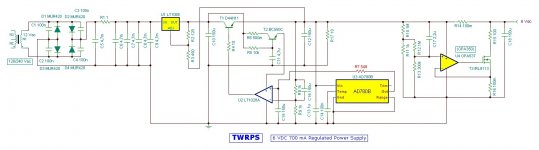
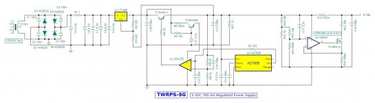
Follows the final schematics of two versions of regulator: HG version is a 6Vdc 700mA with hi-grade components, SG is a 5Vdc 700 mA with standard components.
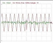
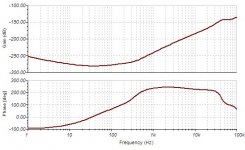
I attach some analisys of HG simulated circuit.
I'm going to order components to build two prototypes.
Andrea
Follows the final schematics of two versions of regulator: HG version is a 6Vdc 700mA with hi-grade components, SG is a 5Vdc 700 mA with standard components.
I attach some analisys of HG simulated circuit.
I'm going to order components to build two prototypes.
Andrea
Attachments
-
 TWRPS-HG.JPG98.3 KB · Views: 1,501
 -
 TWRPS_SG.JPG96.4 KB · Views: 1,430
 -
 Osc.jpg56.7 KB · Views: 1,386
 -
 AC_Transfer_Char.jpg58.2 KB · Views: 910
 -
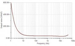 Output_Noise.jpg49.9 KB · Views: 264
 -
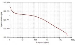 Signal_to_Noise.jpg51.4 KB · Views: 245
 -
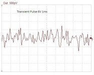 Transient_Pulse_6V_1ms.jpg43.8 KB · Views: 232
 -
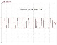 Transient_Square_10mV_120Hz.jpg40.4 KB · Views: 255
I think that cannot work because I need a voltage on the base of D44H11 greater than emitter voltage, so if I supply LT1028 from the final regulated voltage I cannot reach a positive vbe. At least I should replace NPN transistor with a PNP type.
Jung super regulator operate in a different mode, pass transistor is biased from a constat current source and the op amp modulate this current with error signal.
Andrea
You are right, I missed that. It only works when you use a PNP pass.
'
jan
This might be slightly off-topic, in a way, but is probably worth thinking about.
What about simulating with digital loads (e.g. pulsed current draw), and including power and ground rails' impedances, and looking at the voltage across the load? Then everything will depend on the decoupling capacitors at the load.
Typically, it seems that people expend much effort on a power supply but not enough effort on the effects of the impedance of its connections to the load, and the decoupling capacitor networks at the load.
What matters most is what happens at the load, not at the power supply output.
Even with a truly-perfect power supply, any load drawing transient currents through inductive power rail conductors (or planes) will produce voltage disturbances on power/gnd rails (or planes), at the load, with amplitudes of voltage disturbances dependent almost solely on decoupling capacitors and load's transient-current demand's amplitudes and timing.
Decoupling caps at each load are like small point-of load power supplies, for transient current demands. (With a known maximum change in current that might be needed, di, and a known minimum time during which that might have to occur, dt, and a desired maximum voltage disturbance on the power rail (at the load) due to the transient current, dv, which we get to choose, the needed minimum decoupling capacitance can be estimated with C = di dt / dv. There is more to consider, and different ways to look at it, but that, or double that to be safe, is better than just guessing. [You do also have to calculate an estimate of the inductance that can be tolerated in the connections of the caps to the load, to determine their maximum acceptable length and whether or not multiple parallel caps need to be used instead. Simplified way would be L = dv dt / di.])
What is the actual goal? Isn't it for the power pins of the active devices to receive (or give) the current they demand, exactly as needed (amplitude vs time), while the voltage is maintained at a constant value? (Or is the constant voltage value even always necessary, as long as the device pin's current's amplitude vs time is exactly correct?)
I guess low-noise steady-state stuff is relatively easy and well-known. But transient current demands can ruin your best design if you haven't paid very close attention to the rail impedance effects and used optimal decoupling networks very near the points of load. It's still just about as important when using full power and ground planes.
Without power and ground planes: Best way would probably be to have zero-length power rails and a fantastic PSU. Second-best might be to use multiple parallel copies of each voltage and ground rail (lowering overall impedance by paralleling paths, i.e. by having no mutual self-inductance), each path with its own caps at both load and PSU ends and paths all connecting only at a single point at each end. Third best is probably the usual way but to also carefully design the decoupling capacitor networks. You can simulate all of those. Probably nothing else is really worth trying, if performance is critical.
Even when using power and ground planes, with many dispersed decoupling caps around chips, you would probably also want to disperse the power and ground connections to the planes (which is sometimes forgotten), with fully-parallel connections all the way back to the actual main supply and ground points. You could probably simulate a best-case scenario for that, by assuming all decoupling cap currents take separate paths (so no mutual inductance makes inductance reduce fully due to parallel paths), and calculating the overall impedance of the parallel paths.
Sorry to have blathered-on about all of that, for so long.
Cheers,
Tom
In your simulations, you should probably also try including estimates of the parasitics, of both the components and of the conductors. It will give a much-more-realistic simulation (although slower-running), and could also help you to find out which, if any, conductors' lengths might be critical to keep short.
For a first approximation, you can usually use .001 Ohm of series resistance per inch of PCB trace and 30 nH of series self-inductance per inch. (Obviously you might have to guess at, or estimate, the PCB trace lengths, for now.)
If you don't know the parasitic series inductance of a capacitor, then at least include 30 nH per inch of lead spacing. And many resistors have roughly 0.2 pF or so of parallel parasitic capacitance.
The parasitic series resistance (ESR, or Equivalent Series Resistance) of electrolytic capacitors changes quite-significantly, with frequency. If ESR is not given at the frequency you need for simulation, you can usually convert it, using the assumption that the dissipation factor (tan(delta)) varies by much less, versus frequency, usually less than 100% overall. They are related by
tan(δ) = 2 ∙ π ∙ f ∙ C ∙ ESR
which can be used to get tan(δ) if you know only the ESR at a particular frequency.
Then you can solve for ESR and re-calculate the ESR for different frequencies, assuming that tan(δ) doesn't change by much:
ESR = tan(δ) / (2 ∙ π ∙ f ∙ C)
There is usually also a leakage current spec, such as "I = .01 C V or 3 uA, whichever is greater", which should be used to calculate the parasitic parallel resistance, i.e. V/I = R = 1 / (.01 C) .
Although they might be too cumbersome, and are probably unnecessary to use for this project, I should mention that there are ways to make spice models of electrolytic capacitors with ESR modeled such that the effects of any frequency are included. For example, see Cornell Dubilier Plug-In Thermal / Life Calculator , which also nicely displays how various electrolytic capacitor parameters change with temperature and frequency (and will automatically provide a frequency-dependent spice model for any of their electrolytic caps).
Based on a Maxim application note, it can cancel noise up to 1.3 mV. Best choise for op amp should be OPA350, but I'm note sure it can tolerate 6V power supply; data sheet indicates 7V as absolute maximum supply voltage and 5.5V max operating voltage.
So why don't you just use that TI part that the Spaniard discussed.
Use the LM833? It goes from +- 5v to +-18v. I ugess you
wouldn't have to worry about low voltage spikes. ; )
Sync
So why don't you just use that TI part that the Spaniard discussed.
Use the LM833? It goes from +- 5v to +-18v. I ugess you
wouldn't have to worry about low voltage spikes. ; )
Sync
Original application note use a MAX4475 opamp, that has two problems: first it work only up to 6V, but I need an opamp tha work up to at least 30V; second it's an SMD components, and as you see about any other components in the schematics I avoid to use SMD components for this project.
I cannot use LM833 because it has a relatively high input bias current characteristic. As you can see in the application note: "... use an op amp with low input bias current..".
In my simulation that means to use an op amp with ultra low bias current, max 1-2 pA, to work properly, but LM833 has a typical 500 nA ib current.
The OPA637 in the HG schematic is not the cheapest op amp but surely an high performance op amp suitable for this implementation:
input bias current: 1 pA
input voltage noise: 4.5 nV/sqrt(Hz)
slew rate: 135 V/us
gain bandwidth: 80 MHz
AD820 used in the SG version, IMHO is the right price/performance compromise
Up to 5.5V OPA350, in my simulation, it's the best choise for its transconductance, perfect for this feedforward shunt regulator:
input bias current: 0.5 pA
input voltage noise: 5 nV/sqrt(Hz)
slew rate: 22 V/us
gain bandwidth: 38 MHz
Andrea
LM833 is a dual so it's choice is rendered mute. getting to the theory, however, you don't want to use a comparatively slow opamp like the LM833 (16MHz) as the reduced bandwidth increases the effective impedance of the supply. use the fastest opamp you can keep stable. Better are the OPA353, LME49710, AD825 -- but you have to make sure that the regulator remains stable every time you change the opamp.
LM833 is a dual so it's choice is rendered mute. getting to the theory, however, you don't want to use a comparatively slow opamp like the LM833 (16MHz) as the reduced bandwidth increases the effective impedance of the supply. use the fastest opamp you can keep stable. Better are the OPA353, LME49710, AD825 -- but you have to make sure that the regulator remains stable every time you change the opamp.
As i said in the previous post, not all opamp are suitable for this application.
OPA353 is a low voltage opamp and for voltage up to 5.5V the best choise is OPA350, ideal for its transconductance.
LME49710 is a good opamp, but it has an high input bias current (70 nA), too high for this application.
AD825 is a good opamp, but is an SMD device.
BTW OPA637 is an high speed opamp (135V/us), very low noise and ultra low input bias current (1pA), so I thing ideal for this application, and my simulation confirm that. The only problem is the price, so I'll test AD820 in the SG version as a compromise.
Andrea
hmm, so the opa637 is for higher voltage versions yes? its really not very happy with low gain in my experience it needs to be 3-4x or above, certainly not unity
you're right, an unity gain stable opamp in not the ideal opamp, unfortunately OPA350 is a low voltage opamp and I cannot find any valid alternative. I have investigated several opamps in my simulations, but seems all I found suitable for this feedforward shunt regulator are low voltage type. Also AD825 (and I would like to avoid SMD device) does not work properly in this circuit, cause of its relatively high input bias current. Remember that the resistors network divider at the non-inverting input of the op amp must set 1-1.5 mV, so high values resistors are needed, then an input bias current greater than a few pA cause a voltage drop on the resistors.
So I decided to try OPA637 in the first prototype to see if it really has problems like oscillations or so.
Andrea
you could try opa827, its happy at unity gain and equal to 637 in every measure..ah SMD mate that requirement in particular is pretty limiting today. why? dont tell me you are SMD phobic or some other such 'audiophile' nonsense? or you wish to sell it to those who are?
I have nothing against SMD devices, but my eyesight has declined in recent years and so I have a little difficult soldering them.
BTW OPA827 does not work properly in simulation, no problem about input bias current, but I think there are problems about its transconductance.
I'll investigate again among SMD devices.
Andrea
- Home
- Amplifiers
- Power Supplies
- The Well Regulated Power Supply