someone is paying attention.......
"Quite right" My fault for not explaining that it was already part of the regulator. Of course the gate of J202 could also be biased from the filtered output of the LM329 for less noise. If you used a film cap and a large resistor to filter the reference voltage at the op amp, you might have to watch out for the effect of 20 to 30nA of leakage current from the reverse biased diode. A one megohm resistor in this filter would only give you only a few 10s of millivolts error though, and is probably not going to worry too many people. The 5K source resistor and voltage at the gate, would give about 2 to 3 times the output impedance over the J202 without any source resistor. This would be without the extra complexity and expense of a cascode current source. I don't want to over do the circuit either, and a cascoded current source is getting in the realm of the truly exotic for this application. This current source is providing the current to bias a fairly low impedance LED and we are probably below the LED noise floor of a few microvolts for a single jfet current source with a couple of megohms output impedance. It has been very interesting to look so closely at the performance of jfet current sources and LED voltage references. I would like to thank Mr. Curl and Mr. Jung for their thorough analysis of these circuit options. Where else are you going to get stuff this good guys, without paying for pretty specialized consulting? I am pleased for the dialog on a subject that's very interesting to me, and hopefully to others. I appreciate both of these gentlemen's efforts greatly.
Thanks JC and WJ,
Fred Dieckmann
We seem to be convinced that the opamp supply should be derived from the regulated output, which then gets us into all the level shifting and current source discussions (very enlightning).
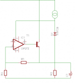
I would like to suggest an alternative method that avoids the level shifter (at least inside the feedback loop). I would welcome your comments on the approach shown in the attachment (apologies I have not yet learned how to insert an image into a post). R3 is probably is not required because the values of R1 and R2 can be adjusted to sink the correct current.
Having one less transistor in the f/b loop may help with stability and transient response. Also the finite current source impedance will affect only the supply to the opamp rather than a hgih impedance point within the feedback loop.
Attachments
hi Walt
the more fundamental question that interests me is how does the super reg compensation work, especially when many diy hackers may hook the super reg up to circuits with 1000’s of uF of local supply bypass C
I scanned the AD825 SPICE model to see if it would realistically model the 4/2000 super regulator circuit because it appears to me that the regulator either relies on the special capacitive load stabilization compensation of the AD825 or the relatively high 1st pole of the open loop gain causing the load Cap*(Requiv op amp+ Q1) to form the dominant feedback pole. Further the super reg has a minor feedback coupling through the PSRR (is the negative voltage version noticably different due to the bootstrapping of the internal compensation cap? Is the AD817 Ccomp referenced to the positive rail instead of the negative rail as is the case with the AD825 and would one be preferred over the other in pos/neg super reg? )
having looked at the AD825 SPICE models, I don't see where the capacitive load gain reduction/stabilization from Cf in the simplified schematic (ad825 datasheet fig 4) is modeled, unless reducing L1 to the physically ludicrous value of 6 pH is supposed to cover it
has anyone at Analog Devices other than Alexander and Bowers read an-138?
certainly few of the apps people you (used to?) let write SPICE models seem to have taken it for a standard to aspire to
Re: POST #469
It depends upon a finite ESR to work. That is why high-Q caps can make it sing if nearby. ESR of 100-200milliohms or more is best, and very low ESR lytics (for example Oscons) can also give trouble, by giving rise to quasi-stability (doesn't oscillate outright, but will ring with step loads).
The regulator is not dependent upon the ad825 or ad817 internal cap load compensation for operation. Many regs have been built with other op amps. That said, I would also say that pole/zero compensated op amps may give trouble, because of their phase funnies (phase margin dips) at HF. See OP27, for example.
I don't believe this part of the ad825's circuit made it to the model, at least it isn't obvious to me that it did. I wasn't involved with the ADI model generation, but I am familiar with the Derek Bowers/Mark Alexander topology, which the ad825 does use. I will forward your comments to the apps folks there at ADI.
wj
the more fundamental question that interests me is how does the super reg compensation work, especially when many diy hackers may hook the super reg up to circuits with 1000’s of uF of local supply bypass C
It depends upon a finite ESR to work. That is why high-Q caps can make it sing if nearby. ESR of 100-200milliohms or more is best, and very low ESR lytics (for example Oscons) can also give trouble, by giving rise to quasi-stability (doesn't oscillate outright, but will ring with step loads).
I scanned the AD825 SPICE model to see if it would realistically model the 4/2000 super regulator circuit because it appears to me that the regulator either relies on the special capacitive load stabilization compensation of the AD825 or the relatively high 1st pole of the open loop gain causing the load Cap*(Requiv op amp+ Q1) to form the dominant feedback pole.
The regulator is not dependent upon the ad825 or ad817 internal cap load compensation for operation. Many regs have been built with other op amps. That said, I would also say that pole/zero compensated op amps may give trouble, because of their phase funnies (phase margin dips) at HF. See OP27, for example.
having looked at the AD825 SPICE models, I don't see where the capacitive load gain reduction/stabilization from Cf in the simplified schematic (ad825 datasheet fig 4) is modeled, unless reducing L1 to the physically ludicrous value of 6 pH is supposed to cover it
I don't believe this part of the ad825's circuit made it to the model, at least it isn't obvious to me that it did. I wasn't involved with the ADI model generation, but I am familiar with the Derek Bowers/Mark Alexander topology, which the ad825 does use. I will forward your comments to the apps folks there at ADI.
wj
I really think the 4/2000 super reg with the AD825 is operating with the output cap and Q1 drive impedance forming the dominant pole;
[[~ 8 Ohm (AD825 Zout) + 10 Ohm (R23) + Rb (Q1) ] / ~100 (hfe Q1) ]+ Re (Q1)
~>/= 0.3 Ohms
0.3 Ohm * 120 uF ~ 30 uS
the AD825 open loop pole is:
2000 (open loop gain) * ~= 8 nS ( from 1/ 2pi*GBW) = 16 uS
the Cout time constant is 2 x the AD825 open loop pole
I wouldn’t consider this approach to have good margin due to with the likely large variability of Hfe and AD825 open loop gain, but increasing ouput Cap C4 by 8-10X is entirely practical and this compensation scheme would work with extremely low ESR caps
A Local (inner loop) feedback could stabilize the AD825 open loop gain pole location, the loop gain loss from setting inner loop to ~ 1000 is small and the reg Zout increase from reduced loop gain is easily made up by increased Cout, the inner loop could also be tailored to control possible strangeness above 1 MHz where the output cap Z is rising and Q1 Hfe roll off begins entering the picture while the AD825 still has gain left
I realize the mods to make this scheme work are well beyond the point of your 4/2000 articles’ use the existing pcb
Re multipole macro models; the AD825 is a simplified version of AN138 and fails to capture the different +/- PSRR in the more realistic way that proportioning pole/zero impedances between the op amp power pins is capable of
also isn’t Cin really fet body-substrate C and should at least be modeled with diodes to capture some of the input Z common mode input nonlinearity
also to jcx
wj: See below for "wj: " comments...
I really think the 4/2000 super reg with the AD825 is operating with the output cap and Q1 drive impedance forming the dominant pole;
[[~ 8 Ohm (AD825 Zout) + 10 Ohm (R23) + Rb (Q1) ] / ~100 (hfe Q1) ]+ Re (Q1)
~>/= 0.3 Ohms
0.3 Ohm * 120 uF ~ 30 uS
wj: Actually the math above yields 36 us, not 30.
wj: And, there is a zero at Resr*C, which is 0.15 * 120e-6 = 18 us. This roughly falls on top the AD825 OL pole. gee... that seems really fortuitous, doesn't it?
the AD825 open loop pole is:
2000 (open loop gain) * ~= 8 nS ( from 1/ 2pi*GBW) = 16 uS
the Cout time constant is 2 x the AD825 open loop pole
I wouldn’t consider this approach to have good margin due to with the likely large variability of Hfe and AD825 open loop gain, but increasing ouput Cap C4 by 8-10X is entirely practical and this compensation scheme would work with extremely low ESR caps
wj: I don't see the logic of this, as your analysis has neglected the cap ESR altogether! This cannot be overlooked. Obviously, as I pointed out earlier it does enter into the picture, and it can influence stability if out of range. And, I actually noted the stability degradation with low ESR caps. A perfect cap would be problematic..... as was also noted before (comment on high-Q caps).
wj: Ahah! Dmitri's post #472 has just arrived, so he has beat me to pointing out your error on neglecting ESR. Thanks for the comments, Dmitri.
A Local (inner loop) feedback could stabilize the AD825 open loop gain pole location, the loop gain loss from setting inner loop to ~ 1000 is small and easily made up by increased Cout, the inner loop could also be tailored to control possible strangeness above 1 MHz where the output cap Z is rising and Q1 Hfe roll off begins entering the picture while the AD825 still has gain left
I realize the mods to make this scheme work are well beyond the point of your 4/2000 articles’ use the existing pcb
wj: Actually, a workable OL compensation *was* discussed in the article, as an option. Did you miss it?
Re multipole macro models; the AD825 is a simplified version of AN138 and fails to capture the PSSR in the more realistic way that proportioning pole/zero impedances between the op amp power pins is capable of
also isn’t Cin really fet body-substrate C and should at least be modeled with diodes to capture some of the input Z common mode input nonlinearity
wj: I don't know where you found the axe to grind here. I don't write the ADI models, and I no longer work for them. I suggest that you write to linear.apps@analog.com, if you feel so strongly about macromodeling sins of omission.
wj
Small cap gains
Mr. Jung raises the excellent point that an output capacitors parasitics sold be part of the design process. I believe this topic has come up on the forum in the past as well. The ESR is often given in the capacitor specs and ESL can be estimated by compare the case size of the cap in question with that of a similar cap who's ESL number is characterized. This level of parasitics analysis is becoming common enough that at least one manufacturer has developed a Spice program for their capacitors.
http://www.kemet.com/kemet/web/homepage/kechome.nsf/vabypagename/spicesoft
Deliberately increasing the ESR of capacitor types such as OSCON Black and film caps can also be achieved with a small series resistor. A parallel array of small low ESR and ESL caps, each having it's own additional resistor could give quite a bit of flexibility in creating the characteristics one might want in this "composite capacitor"
Attachments
How are you doing, Fred?
>Deliberately increasing the ESR of capacitor types such as OSCON Black and film caps can also be achieved with a small series resistor.<
I also use this technique a lot, particularly for bypassing/decoupling duties. In my case, the caps are usually some flavor of stacked film, stacked ceramic or OS, while the resistors are typically low-ohmage SMD or leadless packages.
Without the series resistor, at times you can end up with high-frequency high-Q resonances that may lead to a somewhat etched, forward sound. But different situations can give rise to different resonant behavior (or varying sensitivity to the resonances that do occur), so it also pays to experiment on a case-by-case basis.
regards, jonathan carr
Thanks
Another treat for Halloween from the other JC. I was wondering how long till you got in on this. Thanks for the very useful information. What a great collection of ideas we've managed to trick out of some of the real audio veterans! Remind me to bring a pocket notepad if I ever go drinking with any of you guys. The forum has really become to place I have long hoped for some really good high end audio design hints.
Another treat for Halloween from the other JC. I was wondering how long till you got in on this. Thanks for the very useful information. What a great collection of ideas we've managed to trick out of some of the real audio veterans! Remind me to bring a pocket notepad if I ever go drinking with any of you guys. The forum has really become to place I have long hoped for some really good high end audio design hints.
my point is that there is the possibility of an alternative compensation that allows the use very low esr caps not too "far" from the existing super reg topology/circuit, of course the zero from the esr has to be considered, but i belive my suggestion allows stability with much smaller esr, and allows the "infinite" increase of the Cout that many diy builders tend towards
yes i am finding it hard to find the compensation discussion in the on-line articles i have access to - but then i also have trouble reading off the monitor, maybe time to print it all out...
i should also think anyone here would recognize the "engineering" math; accuracy of calculation beyond the quality of the estimates is pointless, just be sure to round in the conservative direction
i certainly don't mean to badger you on AD's spice modeling, i just wished that OP Amp manufacturers spent an amount of effort on the model proportional to the time their customers end up wasting by using poor models
enjoy your retirement but the name "Walt Jung " will remain associated with Analog Devices in my mind for some time to come
Stability analysis without including ESR?
Would you believe that's already been discussed? See article below, page 16, Figure 5 and the associated box.
Pardon me, but I still don't see how anyone could comment on stability without *explicitly* considering the ESR of the very capacitor under discussion.
I think I mentioned this one earlier (I could be wrong). I built a website after I was inundated with requests to email the AE 4/2000 article. This article can be retrieved at:
http://home.comcast.net/~walt-jung/wsb/PDFs/Improved_PN_Regs.pdf
wj
my point is that there is the possibility of an alternative compensation that allows the use very low esr caps not too "far" from the existing super reg topology/circuit, of course the zero from the esr has to be considered, but i belive my suggestion allows stability with much smaller esr, and allows the "infinite" increase of the Cout that many diy builders tend towards
Would you believe that's already been discussed? See article below, page 16, Figure 5 and the associated box.
Pardon me, but I still don't see how anyone could comment on stability without *explicitly* considering the ESR of the very capacitor under discussion.
yes i am finding it hard to find the compensation discussion in the on-line articles i have access to - but then i also have trouble reading off the monitor, maybe time to print it all out...
I think I mentioned this one earlier (I could be wrong). I built a website after I was inundated with requests to email the AE 4/2000 article. This article can be retrieved at:
http://home.comcast.net/~walt-jung/wsb/PDFs/Improved_PN_Regs.pdf
wj
Mr. Jung raises the excellent point that an output capacitors parasitics sold be part of the design process. I believe this topic has come up on the forum in the past as well. The ESR is often given in the capacitor specs and ESL can be estimated by compare the case size of the cap in question with that of a similar cap who's ESL number is characterized.
Fred, I would change "excellent" to necessary, above. Obviously, from the postings by jcx and yours truly, one cannot just hang any old cap on the output of one of these regs. I believe you talked a little while back about using an Oscon on Andy's card? Be careful with that, for the reasons we've been discussing. A small series R of about 0.5 ohm will do wonders tho, and should restore stability.
wj
Invaluable nuggets of information
Yes, yes, Fred, we are watching and listening very carefully with bated breath for the next really good high end audio design hint.
So can be LED used as a voltage reference? Will such reference generate excess noise as compared with the couple of diodes connected in series? Does somebody have a reliable data?
Y'all are going to kill me for this...
I was reading with interest the discussion regarding the current source, and making its value less sensitive to supply voltage. I'm looking at a SPICE simulation of the 90 Volt version posted here: http://www.diyaudio.com/forums/showthread.php?postid=256528#post256528 I tried several things. I removed the LED biasing resistor and replaced it with an ideal current source. Then I removed the LED and its biasing resistor completely, replacing the LED with an ideal voltage source. I looked at the voltage transfer function from the unregulated input to the output, that is, the small signal AC line rejection, from 10 Hz to 10 MHz. The result? Absolutely no change whatsoever. Kind of like the old Twighlight Zone episode where the doctor shouts "No change!!!" (sorry, you had to have seen it).
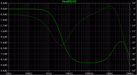
On a slightly different subject, there's been some discussion of the load capacitor and its effect on stability. For the 90 Volt reg, I decided to post a plot of the simulated voltage transfer function from the base of the PNP emitter follower connected to the op-amp output to the output of the regulator itself. As I mentioned before, the load capacitor is 100 uF with a series inductance of 30 nH and a series resistance of 0.25 Ohms. This gives a series resonant frequency of about 93 kHz. Note also that the ESR of the cap is of the same order of magnitude as the open-loop output impedance of the pass element. You can clearly see that the cap interacting with the pass transistor gives the circuit the behavior of a very low-Q notch filter, but with high-end rolloff. That filter has phase lead above the 93 kHz center frequency, which helps the stability situation somewhat. The solid curve is the magnitude and the dotted curve is the phase. For this circuit, you don't want the unity loop gain frequency to be much above 3 MHz or so.
I was reading with interest the discussion regarding the current source, and making its value less sensitive to supply voltage. I'm looking at a SPICE simulation of the 90 Volt version posted here: http://www.diyaudio.com/forums/showthread.php?postid=256528#post256528 I tried several things. I removed the LED biasing resistor and replaced it with an ideal current source. Then I removed the LED and its biasing resistor completely, replacing the LED with an ideal voltage source. I looked at the voltage transfer function from the unregulated input to the output, that is, the small signal AC line rejection, from 10 Hz to 10 MHz. The result? Absolutely no change whatsoever. Kind of like the old Twighlight Zone episode where the doctor shouts "No change!!!" (sorry, you had to have seen it).
On a slightly different subject, there's been some discussion of the load capacitor and its effect on stability. For the 90 Volt reg, I decided to post a plot of the simulated voltage transfer function from the base of the PNP emitter follower connected to the op-amp output to the output of the regulator itself. As I mentioned before, the load capacitor is 100 uF with a series inductance of 30 nH and a series resistance of 0.25 Ohms. This gives a series resonant frequency of about 93 kHz. Note also that the ESR of the cap is of the same order of magnitude as the open-loop output impedance of the pass element. You can clearly see that the cap interacting with the pass transistor gives the circuit the behavior of a very low-Q notch filter, but with high-end rolloff. That filter has phase lead above the 93 kHz center frequency, which helps the stability situation somewhat. The solid curve is the magnitude and the dotted curve is the phase. For this circuit, you don't want the unity loop gain frequency to be much above 3 MHz or so.
Attachments
Andy,
I have two remarks on this very interesting post, if I may.
Firstly, the fact that you can find no difference in the line rejection when changing the input cs configuration. I find that VERY strange. I would accept something counter-intuitive, because such often are the ways of mother Nature, but no change? Really?
On the transfer function curves, I note that the dip of the magnitude is just 8dB or so. Although it does diminish the curative effects of the control loop in that area, 8dB is not dramatic.
Is it too much to ask to run the same simulation but now with an output cap of 1uF, 5nH and .01 Ohms?
Jan Didden
Andy, I have two remarks on this very interesting post, if I may. Firstly, the fact that you can find no difference in the line rejection when changing the input cs configuration. I find that VERY strange. I would accept something counter-intuitive, because such often are the ways of mother Nature, but no change? Really?
Hi Andy. I tend to agree with Jan here. As a SW EE, surely you must have been bitten somewhere along the way by a SPICE blind spot?
")
I suggest backing up and looking at it with a DC sweep, to get the basic feel of what the different topologies do, then go on to the AC. They should be readily differentiated.
Some more general comments on your ckt (which I hope will be helpful).
1) The noise of the high voltage level shifting zeners will be horrendous relative to the Isource noise. I would suggest moving the C3 100uF bypass cap to other side of R7, to make a LP filter that works against 300 ohms vis-a-vis the low dynamic Z of the zeners.
2) Note that this will also have another positive effect, that of attenuating the AC components of the Isource noise. In fact the lower the Z seen at the Isource output, the better off will be everything.
3) You alluded to the Pd of the TL431. Yes, at 30V, it is an issue! Here's a suggestion for you. Couldn't this be helped by dropping the terminal voltage downward? The OP37 op amp (and others) don't require a full 30V to operate. 15V should do fine, and will help the Pd of the 431 by a factor of 2x.
I would think that the relative Z of the Zobel network R17-C5 would have a dramatic effect on phase/gain, in the regions you are targeting.
Hope this is helpful.
wj
Hi guys,
Regarding the simulated line rejection results, please note that I'm not making the claim that these are some kind of ironclad results. It's really just to say, "This is what I found". I'm going to try some more things and see what shakes out. I did have to use a .NODESET directive to get the DC analysis to converge. I need to figure out how to get LTSpice to report the DC operating points it found for the AC analysis.
Walt was right about the Zobel network affecting the results, though it is a bit subtle. The plots without the Zobel network (not shown) show slightly less phase shift at 10 MHz - about -37.5 degrees lag instead of -45 degrees, and -8.0 dB of gain. I found that reducing the Zobel network series capacitance by a factor of 10 still killed the 50 MHz parasitic just fine. That should kill the extra phase lag from this contribution.
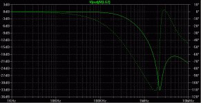
Per Jan's request, I've shown a plot with a load capacitor of 1 uF, having a series resistance of .01 Ohm and a series inductance of 5 nH. The attenuation at the notch is 33.3 dB, which would correspond to an output impedance of the pass transistor of 0.45 Ohms if it were purely resistive. This is consistent with the 61 mA operating current from the DC current source load. The behavior with the 100 uF cap with 0.25 Ohm ESR is also consistent with that value of pass transistor output impedance. I think this plot shows pretty clearly that a low ESR cap is not good. The notch can be so deep that it forces the loop gain magnitude to unity at a frequency below the notch where the phase is lagging considerably.
I would expect the D44H11's to do better here than the MJE15030 I'm using, because of their higher ft. I have done some checking of the simulated ft of the MJE15030 model vs the data sheet curves. They agree well with the data sheets. Those results are shown here http://www.diyaudio.com/forums/showthread.php?postid=245533#post245533 Note that I incorrectly wrote "IKF" in that post when I should have written "ITF", which Christer later caught. Maybe I could get one of the mods to edit this.
I did the plot below by replacing the 100 uF cap with the 1uF cap. I'm now beginning to wonder whether Jan wanted this or to add it in parallel with the 100 uF cap. The Zobel network has been removed for this simulation.
Regarding the simulated line rejection results, please note that I'm not making the claim that these are some kind of ironclad results. It's really just to say, "This is what I found". I'm going to try some more things and see what shakes out. I did have to use a .NODESET directive to get the DC analysis to converge. I need to figure out how to get LTSpice to report the DC operating points it found for the AC analysis.
Walt was right about the Zobel network affecting the results, though it is a bit subtle. The plots without the Zobel network (not shown) show slightly less phase shift at 10 MHz - about -37.5 degrees lag instead of -45 degrees, and -8.0 dB of gain. I found that reducing the Zobel network series capacitance by a factor of 10 still killed the 50 MHz parasitic just fine. That should kill the extra phase lag from this contribution.
Per Jan's request, I've shown a plot with a load capacitor of 1 uF, having a series resistance of .01 Ohm and a series inductance of 5 nH. The attenuation at the notch is 33.3 dB, which would correspond to an output impedance of the pass transistor of 0.45 Ohms if it were purely resistive. This is consistent with the 61 mA operating current from the DC current source load. The behavior with the 100 uF cap with 0.25 Ohm ESR is also consistent with that value of pass transistor output impedance. I think this plot shows pretty clearly that a low ESR cap is not good. The notch can be so deep that it forces the loop gain magnitude to unity at a frequency below the notch where the phase is lagging considerably.
I would expect the D44H11's to do better here than the MJE15030 I'm using, because of their higher ft. I have done some checking of the simulated ft of the MJE15030 model vs the data sheet curves. They agree well with the data sheets. Those results are shown here http://www.diyaudio.com/forums/showthread.php?postid=245533#post245533 Note that I incorrectly wrote "IKF" in that post when I should have written "ITF", which Christer later caught. Maybe I could get one of the mods to edit this.
I did the plot below by replacing the 100 uF cap with the 1uF cap. I'm now beginning to wonder whether Jan wanted this or to add it in parallel with the 100 uF cap. The Zobel network has been removed for this simulation.
Attachments
- Status
- This old topic is closed. If you want to reopen this topic, contact a moderator using the "Report Post" button.
- Home
- Amplifiers
- Power Supplies
- Super Regulator, collecting the facts