The problem you get with transformer based current injectors is that they get saturated pretty quickly (unless it's a really, really expensive transformer) -- you're running the AC + DC current through it.
Yep. That's my guess on what happened as well.
Had you seen Jan's article on the "T-Regulator" from Elektor March 2009
I did see the article. As I recall, it's a floating regulator -- not unlike my HV Reg 3.2, in fact. The T-Reg uses a pair of BJT's for the error amp as I remember. Such a regulator works pretty well as long as you can keep the reference voltage clean. That was the fundamental limitation in my design as far as ripple rejection goes, and I suspect it is in Jan's as well.
~Tom
Hey there, anyone in germany up for sharing shipping cost?
PM me...
ich würde bestellen und dann weiterleiten, um versandkosten zu sparen
Yurgs
European distributor! Great initiative. Thanks.
The shipping cost from the US to any international destination is $18 flat fee regardless of the number of boards purchased. So the distribution model should work pretty well if you can get a handful of people together in a group buy.
~Tom
Is there any reason I couldn't use this regulator after the silicon ray tube smps?
RTP-15 Switching Mode Power Supply (SMPS) for Tube Amplifier - Boards | Kits | Components | Modules | Tools
Great design, I may try modding my zen select to try to use this regulator.
RTP-15 Switching Mode Power Supply (SMPS) for Tube Amplifier - Boards | Kits | Components | Modules | Tools
Great design, I may try modding my zen select to try to use this regulator.
Is there any reason I couldn't use this regulator after the silicon ray tube smps?
Great design, I may try modding my zen select to try to use this regulator.
Thanks. I like my design as well...
")
Whether you can power the Universal Filament Regulator using the Silicon Ray supply or not depends on the output voltage that you desire. If you're aiming for filament voltages of 3.5 V (maybe 4 V) or below, you can run the regulator off of one 6.3 V output. For other filament voltages (up to near 10 V) you'll need two 6.3 V outputs in series. My Universal Filament Regulator is a buck (step-down) converter, hence, this limitation.
I strongly suggest using WebBench or my recommended values spreadsheet to confirm that the regulator will work for you.
~Tom
hi tom,
i've looking for a HV regulator for a few weeks. every time i google about it this topic and your website hits the search. i'm not an audio guy, but i like your design and i'm a fan for obselete MC1466 which is ancestor of LT3080. i'm thinking about to make a HV power supply. maximum output voltage may be 900-1000V. but it must be adjustable in full range, ie 0-900V. also, floating output and short circuit protection is needed. as max nominal output current 10mA is enough for me. i'll use this PS for electrostatic deflection as in the CRT tubes. is it possible to use your design for my purpose? furthermore, consider to using a R-2R DAC as set input of LT3080. so that, an external voltage can control the output. what do you think about this?
i've looking for a HV regulator for a few weeks. every time i google about it this topic and your website hits the search. i'm not an audio guy, but i like your design and i'm a fan for obselete MC1466 which is ancestor of LT3080. i'm thinking about to make a HV power supply. maximum output voltage may be 900-1000V. but it must be adjustable in full range, ie 0-900V. also, floating output and short circuit protection is needed. as max nominal output current 10mA is enough for me. i'll use this PS for electrostatic deflection as in the CRT tubes. is it possible to use your design for my purpose? furthermore, consider to using a R-2R DAC as set input of LT3080. so that, an external voltage can control the output. what do you think about this?
Good to hear that my website is popular with the search engines...
In my design, the input voltage is limited by the input cap and the cascode device, Q1. I wouldn't go much beyond 800 V input with the values I have in the schematic. And not beyond 575~600 V on the output voltage. But I don't see any reason you couldn't use the topology of my design for higher voltages.
On the topic of current limiting, see my earlier post on the topic.
~Tom
MOSFET SOA problems
I have been trying to build the design from this thread for a target output of 500V at 500mA approx. for a KT88 parallel push pull amplifier and have come up against many problems.
As far as I can see any linear regulator using recent MOSFET designs other than a very few specific devices will probably fail if the pass element exceeds as few tens of watts dissipation at any time during start-up.
I am not an expert in power electronics but it appears that the extreme optimisation of MOSFETs for switching applications has caused them to become unable to function at even moderate currents at high voltages as the devices have a positive temperature coefficient when operated in linear mode (this means the saturated region of the MOSFET characteristic).
A good description of this topic is found in: http://www.ixys.com/Documents/AppNotes/IXAN0068.pdf or search for 'MOSFET FSBOA' (forward bias safe operating area).
Here’s how I figured out (dumbly and slowly) what was going on …
I first of all tried building a Swenson / Gary Pimm regulator for 500V 500mA and after a cup full of dead MOSFETs turned to the 21st Century Maida design. Same result; my confusion was immense as I was using 24A 800V 600W (!) IXFH 24N80P pass devices (and the TO220 version of the LDO) and as a test load 2 off 60W 240V light bulbs in series (i.e. a 250mA load at 480V output). I looked for RF oscillations, and pondered LTSpice models to no avail.
Trying different loads start-up into anything above a few 10’s of watts of light bulb caused the pass MOSFET to fail for any Vin over 400V. Improving the thermal interface to the large fan cooled heat sink I was using for testing helped – I did this by removing the insulating pad (not a long term plan!), cleaning the heat sink and MOSFET mounting surfaces, using the right size bolt and a big washer and a torque wrench to avoid deforming the transistor package. This got me to being able to start-up at 240V out with 300V in into a single 60W light bulb with the IXFH 24N80P, but at any voltage above that the pass device would fail.
I then theorised that in some way the current limit circuit wasn’t working and hence a current spike on start-up was frying the MOSFET (although I could not see how), or that the gate was getting spiked despite being protected by a Tranzorb diode. Looking at the voltages across the MOSFET on start-up with a high voltage differential probe provided the answer; the MOSFET was breaking down a few hundred milliseconds into start-up at around Id=100mA, Vds=300V with single digit volts Vdg - a power level of only 30W for a 600W device..! At first I suspected a faulty device and tried another batch of IXFH 24N80P’s and then a different MOSFET of similar specification with similar results.
I then discovered the IXYS application note posted, and product advisories from International Rectifier and others setting out the same problem, which the semiconductor fabricators appear none too keen to publicise. Vendors either now don't publish SOA curves for power MOSFETS or if they do they show serious derating for DC operation to no more than 5-10% of theoretical maximum dissipation regardless of case temperature! The problem is according to the various published studies caused by recent (last few years) changes in device geometries.
I thought about IGBTs briefly as an alternative route and then discovered these are even less well understood operating at DC than MOSFETS.
The same IXYS documentation that explained what was going on pointed me to their ‘L’ and L2 ranges of devices as being designed specifically for linear mode operation. The (very expensive ) IXYS IXTK22N100L is specified for substantial dissipations in linear mode and I have now built a (Swenson) regulator using this device which happily starts up into light bulbs and other difficult loads etc at my target power levels. I incidentally want this to work in case the amp is power cycled with hot tubes. In the production build I will use two of these devices paralleled on an earthed fan cooled heat sink with a high performance silicone insulator pad.
Some of the MOSFETS I experimented with also showed very strange partial failure modes – ‘dying’ in the sense that they would go into continuous conduction and then recovering when power-cycled but failing shortly afterwards - spooky eh? I think these failures come about from the fact that all big MOSFETS consisting of many parallel devices, some of which go short-circuit in the initial failure and others of which continue to work. The positive tempco which underlies the problem of linear mode operation means that the hotter devices on the die get more current, and hence the failure of the whole device follows progressively.
Incidentally anybody out there trying to build something like this - wear safety glasses. A number of the MOSFETs detonated quite impressively with lots of flying plastic and device legs.
I've also now build the 21st Century Maida design with the IXYS IXTK22N100L and it works fine too starting up into difficult loads.
it must be adjustable in full range, ie 0-900V. also, floating output and short circuit protection is needed. as max nominal output current 10mA is enough for me.
You need a quiet h.v. switching regulator -- the late Jim Williams of Linear Technologies wrote an application note for this, and made a video which is on youtube. https://www.youtube.com/watch?v=e9RX_UPownc
I have been trying to build the design from this thread for a target output of 500V at 500mA approx. for a KT88 parallel push pull amplifier and have come up against many problems.
As far as I can see any linear regulator using recent MOSFET designs other than a very few specific devices will probably fail if the pass element exceeds as few tens of watts dissipation at any time during start-up.
As you point out, you have found the SOA limits of your MOSFETs. I was in the same boat when I started building regulators. You can dig through the earlier pages in this thread for more detail.
Basically, the issue is that many loads - in particular capacitive ones - present a short circuit on the output of the regulator at start-up. This causes tremendous power to be dissipated in the cascode MOSFET, which in many cases leads to the premature death of an expensive MOSFET.
The current limiter does help, though. However, the cascode will need to handle the full power of Vin * Ilimit for a short amount of time. This is where you run into problems with high voltage, high current designs. I spent quite a while pouring over SOA curves in data sheets and simulating in LTspice before settling on the STW... device I list in the BOM.
So yeah... What you describe is completely normal in high power designs. Welcome to the club...
In your case, I would suggest running two regulators, 250 mA each. That would allow you to set the current limiter lower, giving the MOSFETs a better chance of survival.
I've also now build the 21st Century Maida design with the IXYS IXTK22N100L and it works fine too starting up into difficult loads.
Thanks for sharing. It's good to hear that you were able to make it work.
~Tom
Hi Tom,
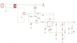
I´m wondering about the wattage of R1/R3 and R9 found in the latest schematic from 26th march 2012.
R1 ( 100K/2W ) will "see" Vin-Vout-10V. To reach round about 2W on 100K UR1 must be 447V. I can´t imagine when this can happens.
For R3 (15R/2W) a current of 365mA is need to reach 2W at R3.
R9 (200K/3W) will need not more than 1W because on 430V Vout you will get only 0.92W.
For my point of view only R3 need to be a "big" resistor with 2W if you realy want to flow current of more than 250-350mA.
Can you explain why you dimension R1 and R9 in such a way?
Thanks a lot
Karsten
Hi Karsten,
he might just be cautious and rates the resistors conservatively.
I try to overrate resistors by 2-3 times of the actual dissipated power - this way they stay reasonably cool.
With the max. allowed power, resistors tend to get unpleasantly hot - in fact way too hot for most capacitors that might be nearby.
I guess this is what Tom did, too, but you might want to hear it from the horses mouth (so to say).
Best,
Martin
I´m wondering about the wattage of R1/R3 and R9 found in the latest schematic from 26th march 2012.
R1 ( 100K/2W ) will "see" Vin-Vout-10V. To reach round about 2W on 100K UR1 must be 447V. I can´t imagine when this can happens.
For R3 (15R/2W) a current of 365mA is need to reach 2W at R3.
R9 (200K/3W) will need not more than 1W because on 430V Vout you will get only 0.92W.
Can you explain why you dimension R1 and R9 in such a way?
Most modern power resistors are made from materials that can tolerate very high temperatures. That's how a 2 W modern resistor can be the size of a 1 W or 0.5 W from "back in the day". If the resistor is dissipating the rated power, it will get screaming hot. As in 200~250 deg C. That's too hot for comfort in my opinion.
In my setup, using the values indicated in the schematic, the resistors typically heat up to around 80~100 deg C (measured with an IR thermometer). This with the regulator sitting out in the open on a piece of plywood in my living room (don't do this at home kids!)
I tend to go with a 4~5x safety margin on power resistors. I might go as low as 3x if the 4~5x gets me into ridiculous resistor wattages.
Just for reference, aerospace and military designs generally use a 10x derating factor. They've done a lot more math on the subject than I have. Just sayin'...
R1 is a 2 W type, because during start-up into a capacitive load, this resistor actually sees the full input voltage across it (well, technically V(R1) = Vin - Vzener, but Vzener is tiny in comparison to Vin). To handle this peak power, a 2 W type is needed, even though it only sees a few tens of mW during normal operation.
Hope this answered your questions.
~Tom
Last edited:
Hi Bayermar, Hi Tom
Thanks for your explanation. To sum up the choosen wattage of the power resistors is done for robustnes and lower temperatur only.
Yepp, seemed to me the right way but unfortunately I have only 80x100mm PCB size for the whole PSU including a EL48 transformer. So I must be carefully choose size and place of potential hot devices.
Well, my PCB will not be a part of an aerospace but why not to try to do it in the same way
Thanks a lot for your hints,
regards
Karsten
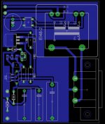
Hi folks,
First try of routing a 80x100mm PCB. It´s designed to feed only 15-20mA on 200 - 300 V for small preamps. Its only single sided and use also a few SMD´s. If it works I will provide you the eagle .brd and .sch schematic
Have fun,
Karsten
First try of routing a 80x100mm PCB. It´s designed to feed only 15-20mA on 200 - 300 V for small preamps. Its only single sided and use also a few SMD´s. If it works I will provide you the eagle .brd and .sch schematic
Have fun,
Karsten
Attachments
Tom, what is the dropout of this regulator? Have you tested it at high voltage, high current and low Vin-Vout? Like on the order of 10V? I don't see anything obvious beside the LT chip dropout and series (limiter) resistor, but I thought I'd better check with the designer
I have tested with 400 V, 225 mA out and dialed the variac on the mains input down to the point where the regulator lost regulation. This tends to happen around 410~415 V DC in a setup with a few volt ripple. So the drop-out is on the order of 10~15 V. I recommend that people design for a worst case drop-out of 20 V to have some margin. The spreadsheet I have on my website does all the necessary math for you.
The drop-out is mostly determined by the zener bias, D2, on the cascode.
~Tom
The drop-out is mostly determined by the zener bias, D2, on the cascode.
~Tom
- Home
- Vendor's Bazaar
- 21st Century Maida Regulator