For 78xx 79xx linear regulator the board is way too big.
It depends on what power youre wasting in those - how big heatsink you need, but anyway I´m sure you can make the vertical dimension just the size of C2+C1.
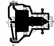
Other than that, post a schmatic, because I can´t see which connector is output and which is input. Anyway AFAIK these linear regulators need two small caps each, not one, If C1 and C2 are output caps then they seem pointless to me, if they are input caps then what do D1 and D2 do? Are they preregulation zeners? Then where are the series resistors?
It depends on what power youre wasting in those - how big heatsink you need, but anyway I´m sure you can make the vertical dimension just the size of C2+C1.
Other than that, post a schmatic, because I can´t see which connector is output and which is input. Anyway AFAIK these linear regulators need two small caps each, not one, If C1 and C2 are output caps then they seem pointless to me, if they are input caps then what do D1 and D2 do? Are they preregulation zeners? Then where are the series resistors?
Hi, and thanks a bunch for your reply.
I'll try to see if I can make it smaller than what it is for now..
Actually the left connector is the input and the right one os the output.
What do you mean 2 caps really plz? The 2 small caps are valued as 104...
C1 and C2 are pointless?!! but way are you thinking so? they actually are the output caps but plz why do you think that they should not be used there?!
As I said the c1 and c2 are the output caps. The diodes are 1N4001 and are used there to do not let the back EMF's and so on to harm the regulator chips...
For 78xx 79xx linear regulator the board is way too big.
It depends on what power youre wasting in those - how big heatsink you need, but anyway I´m sure you can make the vertical dimension just the size of C2+C1.
I'll try to see if I can make it smaller than what it is for now..
Other than that, post a schmatic, because I can´t see which connector is output and which is input.
Actually the left connector is the input and the right one os the output.
Anyway AFAIK these linear regulators need two small caps each, not one,
What do you mean 2 caps really plz? The 2 small caps are valued as 104...
If C1 and C2 are output caps then they seem pointless to me,
C1 and C2 are pointless?!! but way are you thinking so? they actually are the output caps but plz why do you think that they should not be used there?!
[/QUOTE]if they are input caps then what do D1 and D2 do? Are they preregulation zeners? Then where are the series resistors?
As I said the c1 and c2 are the output caps. The diodes are 1N4001 and are used there to do not let the back EMF's and so on to harm the regulator chips...
See this for starters, page 9. http://www.national.com/profile/snip.cgi/openDS=LM78M05What do you mean 2 caps really plz? The 2 small caps are valued as 104...
These two caps per regulator should be placed close to the regulator.
The board traces from input should first go to the cap, then from the cap to the input of the regulator.
I assume you have a bridge rectifier and large electrolytics prior to this board, these caps are the smoothing caps. Placing large capacitance like C1 and C2 on the OUTPUT of the regulator is just asking for problems, because you 1) temporarily short the regulator on startup, 2) hinder it's transient response (caps oppose voltage transients)C1 and C2 are pointless?!! but way are you thinking so? they actually are the output caps but plz why do you think that they should not be used there?!
Ok these diodes have their place there. You should not use any large caps on the output, just the recommended 100nF.As I said the c1 and c2 are the output caps. The diodes are 1N4001 and are used there to do not let the back EMF's and so on to harm the regulator chips...
Ok these diodes have their place there. You should not use any large caps on the output, just the recommended 100nF.
Thanks for your reply.
But most of people use 100/220uF caps at the output of the 78/79xx chips amd recomend to do it!
A finer point would be that you should always keep the power and ground traces/conductors (and ALL conductor pairs) as close together as possible, to avoid creating "enclosed loop area", which acts as an antenna (receiving and/or transmitting) for time-varying magnetic and electromagnetic fields, of which there will be plenty. (See "Faraday's Law", or Maxwell's Equations.)
Thanks for your reply.
But most of people use 100/220uF caps at the output of the 78/79xx chips amd recomend to do it!
The datasheet says 100nf on input and output. If there is something noisy in the circuit then that should be decoupled locally.
A finer point would be that you should always keep the power and ground traces/conductors (and ALL conductor pairs) as close together as possible, to avoid creating "enclosed loop area", which acts as an antenna (receiving and/or transmitting) for time-varying magnetic and electromagnetic fields, of which there will be plenty. (See "Faraday's Law", or Maxwell's Equations.)
Hi, and thanks.
What do you really mean by "conductor pairs"? I though that the enclosed loop problem is just for ground or each trace itself, now you seem to say that it happens between pairs too (for instance between VCC trace and ground)!
Furthermore plz how it acts as an antenna!?
It would be ok if you could plz show me what you are meaning by a pic...
Thanks again
Last edited:
The datasheet says 100nf on input and output. If there is something noisy in the circuit then that should be decoupled locally.
But plz google the schematics for the 78/79xx regulators. MOST of them have big caps at their outputs....
Like this? First 7805 supply on google. http://www.circuitstoday.com/5v-power-supply-using-7805
Big cap on input, small caps near regulator.
Big cap on input, small caps near regulator.
Hi, and thanks.
What do you really mean by "conductor pairs"? I though that the enclosed loop problem is just for ground or each trace itself, now you seem to say that it happens between pairs too (for instance between VCC trace and ground)!
Furthermore plz how it acts as an antenna!?
It would be ok if you could plz show me what you are meaning by a pic...
Thanks again
Google Faraday's Law.
In practical terms, for the layout you gave, just make the distance between the power rails and the large copper ground area as small as possible, everywhere. And twist tightly together any wire pairs that go from or to the board, and everywhere else in your power supply and other circuits.
It will also be very important for things like input signal and signal ground pairs. Either twist tightly together, all the way from input jack to input resistor, or, even better, use shielded twisted pair with shield connected to chassis (NOT signal ground to chassis!) at input end and not connected to anything at other end. Signal ground conductor connects ONLY at the input and at the ground end of the input resistor of the first amplification device (which then has a conductor of its own that goes to the main star ground point. i.e. the input jack (both signal and signal ground portions), must be completely isolated (electrically insulated) from the chassis.
Last edited:
But plz google the schematics for the 78/79xx regulators. MOST of them have big caps at their outputs....
And you would believe "most schematics" instead of believing the manufacturer's datasheet?!
You should probably read several different linear regulator datasheets from each of several different manufacturers. ALSO, search their websites for Application Notes about linear regulators. Sometimes, they might say that you could use a somewhat-larger capacitor at the regulator's output, but they almost always mention, in some way, that it shouldn't be "too large".
Unless you have a proper mathematical justification, just follow the recommendation on the manufacturer's datasheet for the exact device that you are using.
If you are going to use a capacitor on the load side of a regulator, then you would want to place it as close as possible to the point of LOAD, where it can do the most good. And often or usually you would want to have both large and small capacitors at the point of load, e.g. some electrolytic and some small ceramic such as 0.1 uF. ("What C values?", you ask. Ideally, the capacitors' self-resonant frequencies will cover the frequencies of the currents demanded by the load. Caps' self-resonant freqs depend on C values and caps' parasitic inductances and the trace's parasitic inductance. If in doubt, first try 10 uF electrolytic in parallel with 0.1 uF X7R ceramic, at each chip power pin, to ground. Larger current demands would need larger than 10 uF. Higher frequencies would need lower than 0.1 uF.)
But still you have to be careful that none of those capacitances will form an unwanted high-frequency resonance with either the trace inductance or the inductance of any of the capacitors. Lossy capacitors are sometimes best.
Hi, and thanks.
What do you really mean by "conductor pairs"? I though that the enclosed loop problem is just for ground or each trace itself, now you seem to say that it happens between pairs too (for instance between VCC trace and ground)!
Furthermore plz how it acts as an antenna!?
It would be ok if you could plz show me what you are meaning by a pic...
Thanks again
You PCB would be much better if you would use a two-sided board and use the entire bottom side as a ground plane. You would only need to etch small areas on the bottom ground-plane side that were below a through-hole pad that would be soldered on the top side. (OK, you might need a couple of very short traces on the bottom side, for the large capacitors, unless you can angle them enough, or lay them on their sides or something, to enable soldering two of their leads on the top side of the board. And the jacks might need some short bottom-side traces to get to vias next to them, unless you used right-angle jacks.)
Last edited:
marce
Thanks for the links.
Briefly went through the first, one area where I dont typically comform is the placing bypass caps on the same layer as the active parts and avoiding via's.
For me the added via inductance is still near the capacitors ideal self inductance and being able to place them elsewhere clears up the critical io routing. This can be done with ground and power planes, then I am able to place the connecting via's right at the active components power leads. Even without power planes I still find that I am able to better able to keep the supply impedance lower out to higher frequencies with large traces on the bottom side (especially since the by-pass capacitors spacing can then more easily straddle power leads, in the absence of planes).
This is just a practical situation that I seem to run into all the time.
Hope this helps
-Antonio
Henry Ott, page 458")
Most of my data is in PDF form with my CAD libaries so I can access the info readily,
at the moment I have to use a DVD to back this lot up! So I am trying to do some housekeeping and checking documents for updates etc, as I have been collecting this stuff for years (including magazines such as Printed Circuit Design and Fabrication and SMT) and as I am rather disorganised its a bit of a long term project... But here is a zip of a collection of PCB related links including soem good Signal Integrity sites that you may find useful.
One day I will get organised...
Attachments
78/79 regulators are not the best by today's standards, but that was not your question.
Let me be very contrary: There is no such thing as ground, just a place arbitrarily designated as a circuit reference point. There is no magic in shape. You should treat the source and sink with the same diligence. My habit is to use double side board and make the top all ground. This gives me more space to deal with V+ and V- on the bottom side and a cleaner, more straight, and more compact layout. ref: comment by gootee.
Let me be very contrary: There is no such thing as ground, just a place arbitrarily designated as a circuit reference point. There is no magic in shape. You should treat the source and sink with the same diligence. My habit is to use double side board and make the top all ground. This gives me more space to deal with V+ and V- on the bottom side and a cleaner, more straight, and more compact layout. ref: comment by gootee.
- Status
- This old topic is closed. If you want to reopen this topic, contact a moderator using the "Report Post" button.
- Home
- Amplifiers
- Power Supplies
- Ground pplane