Hi All,
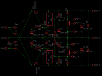
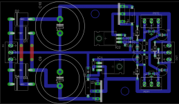
I'm a bit of a newbie, just starting to play with cadsoft eagle and trying to understand electronics fundamentals. The attached pictures are of a PCB design by myself for a dual tracking adjustable Power Supply I've designed for myself. The objective was to learn more about the software package itself as well as come up with something I can make into a bench power supply, or as I understand it, something I could use as a power supply for a class A amp. Forgive the relative untidiness of the schematic, but tidying it up would have involved doing the pcb all over again as an end result!
The schematic is a composite of the psu's decribed at Variable Dual Lab Power Supply the psu kit from jaycar and a cheat sheet example from altronics.
As I understand it, this should be good for upto 37V and 4A.
The Blocks marked POT1 and 2 are for attaching a 20k linear dual gang pot, for adjusting the voltage and the large blank spaces behind the TIP2955 and TIP3055 are for heatsinks, or preferably to lay them flat and share a heatsink with the LM317.
So I've a number of questions I'd hope that someone could help me with.
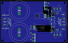
1) layout. I've read loads about optimal layout, and done my best to follow what I've read. Any suggestions for improvements? Er actually, is it even correct?
2) The Capacitor C4 - should it be as close to the ADJ pin of the LM317 as possible, or is it fine where it is. uh, the only reason I ask is that it looks tidier there")
3) the join between pins 2 of the TIP and pin 2 of the LM3*7. The tab on the TIP is the collector, and the tab on the LM is the V-OUT (I hope ) is there any reason not to electrically connect them via the heatsink as opposed to a trace on the board? It'd make the layout a little easier!
4) output capacitance. If it were to be used as a Class A amp PSU, does it need more capacitance at the output? If it were to be used for a class AB PSU would it need more capacitance? I read somewhere that raising the value of the output cap can negatively affect the performance of the LM3*7...
5) how do you get the blasted gap between the traces and the ground plane wider? I don't fancy my chances of home etching the teeny tiny gaps currently there...
6) Any other input? I'll try and upload the eagle files to somewhere that's accessible should anyone want to change the design. I won;t flatter myself that it'll be useful to anyone as yet
I'm a bit of a newbie, just starting to play with cadsoft eagle and trying to understand electronics fundamentals. The attached pictures are of a PCB design by myself for a dual tracking adjustable Power Supply I've designed for myself. The objective was to learn more about the software package itself as well as come up with something I can make into a bench power supply, or as I understand it, something I could use as a power supply for a class A amp. Forgive the relative untidiness of the schematic, but tidying it up would have involved doing the pcb all over again as an end result!
The schematic is a composite of the psu's decribed at Variable Dual Lab Power Supply the psu kit from jaycar and a cheat sheet example from altronics.
As I understand it, this should be good for upto 37V and 4A.
An externally hosted image should be here but it was not working when we last tested it.
An externally hosted image should be here but it was not working when we last tested it.
The Blocks marked POT1 and 2 are for attaching a 20k linear dual gang pot, for adjusting the voltage and the large blank spaces behind the TIP2955 and TIP3055 are for heatsinks, or preferably to lay them flat and share a heatsink with the LM317.
So I've a number of questions I'd hope that someone could help me with.
1) layout. I've read loads about optimal layout, and done my best to follow what I've read. Any suggestions for improvements? Er actually, is it even correct?
2) The Capacitor C4 - should it be as close to the ADJ pin of the LM317 as possible, or is it fine where it is. uh, the only reason I ask is that it looks tidier there
3) the join between pins 2 of the TIP and pin 2 of the LM3*7. The tab on the TIP is the collector, and the tab on the LM is the V-OUT (I hope
) is there any reason not to electrically connect them via the heatsink as opposed to a trace on the board? It'd make the layout a little easier!4) output capacitance. If it were to be used as a Class A amp PSU, does it need more capacitance at the output? If it were to be used for a class AB PSU would it need more capacitance? I read somewhere that raising the value of the output cap can negatively affect the performance of the LM3*7...
5) how do you get the blasted gap between the traces and the ground plane wider? I don't fancy my chances of home etching the teeny tiny gaps currently there...
6) Any other input? I'll try and upload the eagle files to somewhere that's accessible should anyone want to change the design. I won;t flatter myself that it'll be useful to anyone as yet
Attachments
Last edited:
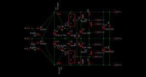
I can't get the two image links at the top of your post to display so my question here is probably answered in those. I'm puzzling a bit at how Q1 will work by itself as a PNP without having it also control an additional NPN bypass pointed as an emitter follower, as in p. 17 of the LM317 data sheet:
http://www.national.com/profile/snip.cgi/openDS=LM317
Same comment with Q2 on the negative rail.
With the emitter follower I can see how the current bypass around the regulator would still be sensitive to the load. But with only the PNP the transistor will just be "on" at a certain point and insensitive to the load, or at least so it seems, and I can't quite see how the regulator would make up for the part in the middle.
Up to 0.65V/3.3R = 200mA through R1 Q1 will be off and all the current will go through the LM317. Great. But then at 1.8V/3.3 = 550mA through R1 Q1 is "on" at the full 4 amps according to the TIP2955 data sheet. The total output current would be the 4A through Q1, 550mA through R1 and 100mA of Q1 base current for a total of 4.65A, so for 4A total the R1 drop would be something like 1.6V.
http://www.onsemi.com/pub/Collateral/TIP3055-D.PDF (Vbe(on) = 1.8V with Vce = 4V and Ic=4A)
What happens between those two points is what I'm not clear about - not seeing how the regulator can adjust adequately enough for the PNP bypass. I'm probably just missing it, but please elaborate! Looks like an interesting circuit. Thanks.
Last edited:
Well... here is a thread from 2004 that says your design will work just fine. See post #15 and #16.
http://www.diyaudio.com/forums/solid-state/41858-current-boost-lm317-prob.html
http://www.diyaudio.com/forums/solid-state/41858-current-boost-lm317-prob.html
Last edited:
Cheers, that's helpful. Well, I've tidied up the pcb a little more and I reckon I'm good to go. I guess I'll just build it and see where I get to. Hopefully there's no drama's! I am curious to know what I'd need to change to make it a suitable Class A PSU, but for now I guess I'll use it to test a few amps and see how I get on.
Hi aspringv, could you post the updated pcb at a bit higher resolution please the first one isn't showing the etched parts of the board very clearly and I'm unsure what's connected to where
1st a disclaimer, I'm probably just as much of a newbie to PS design as you are and more of one when it comes to layout!!
on point 1) have a read of this post http://www.diyaudio.com/forums/power-supplies/184068-psu-rc-multistage-filtering-2.html#post2487825 and then have a look at where your R2 and R5 are. you may want to consider moving the end that is on the output of the reg as close to the reg as you can.
3) I'm not sure if using the sink to electrically attach the output transistor and the LM317 output is a great idea, my biggest concern would be whether it would be the lowest resistance option. 2nd concern is I've blown things up before that had live heat sinks!! to0 easy to touch something you shouldn't, even a glance with the multimeter probe!!
4) for a class A amp the current draw should be pretty much constant, I can't see a bigger output cap making any significant difference here. For a class A/B the current draw will depend on the signal and vary, a bigger cap may be of use, but many claim it doesn't let the regulator do its job properly.
On the negative effect of a bigger output cap, larger capacitance is unlikely to be the actual cause. I would hazard a guess that the real issue is that bigger caps have lower ESR and the LM317's inherent output inductance can resonate with the output cap if there is not enough ESR present to damp that resonance, with a really big cap (eg 1000uF) this resonance will quite likely be in the audio spectrum!. In my design I've included a 0.33ohm series resistor in series with the output cap to ensure this isn't an issue. The datasheet has this to say about the size of the output cap:
5) no idea!
6) nothing I can think of at the moment
Tony.
the first one isn't showing the etched parts of the board very clearly and I'm unsure what's connected to where 1st a disclaimer, I'm probably just as much of a newbie to PS design as you are
and more of one when it comes to layout!! on point 1) have a read of this post http://www.diyaudio.com/forums/power-supplies/184068-psu-rc-multistage-filtering-2.html#post2487825 and then have a look at where your R2 and R5 are. you may want to consider moving the end that is on the output of the reg as close to the reg as you can.
3) I'm not sure if using the sink to electrically attach the output transistor and the LM317 output is a great idea, my biggest concern would be whether it would be the lowest resistance option. 2nd concern is I've blown things up before that had live heat sinks!! to0 easy to touch something you shouldn't, even a glance with the multimeter probe!!
4) for a class A amp the current draw should be pretty much constant, I can't see a bigger output cap making any significant difference here. For a class A/B the current draw will depend on the signal and vary, a bigger cap may be of use, but many claim it doesn't let the regulator do its job properly.
On the negative effect of a bigger output cap, larger capacitance is unlikely to be the actual cause. I would hazard a guess that the real issue is that bigger caps have lower ESR and the LM317's inherent output inductance can resonate with the output cap if there is not enough ESR present to damp that resonance, with a really big cap (eg 1000uF) this resonance will quite likely be in the audio spectrum!. In my design I've included a 0.33ohm series resistor in series with the output cap to ensure this isn't an issue. The datasheet has this to say about the size of the output cap:
from the national semiconductor LM317 datasheet.Although the LM117 is stable with no output capacitors, like
any feedback circuit, certain values of external capacitance
can cause excessive ringing. This occurs with values between
500 pF and 5000 pF. A 1 μF solid tantalum (or 25 μF
aluminum electrolytic) on the output swamps this effect and
insures stability. Any increase of the load capacitance larger
than 10 μF will merely improve the loop stability and output
impedance.
5) no idea!
6) nothing I can think of at the moment
Tony.
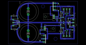
Next Version
...Actually that took way less time than I thought it would.
Diodes uprated to 6A units that I can buy down the road. Relevant caps and resistors moved as close to the regs as possible. No changes made to the type of caps as I couldn't see the point after I thought about it for a while
Feedback appreciated.
Attachments
The spacing of the ground plane in Eagle can be adjusted by setting the clearance in the Isolate box that appears at the second from the right at the top after you hit the polygon key.
Ground Plane Tutorial
AMZ - Eagle groundplane tutorial
Ground Plane Tutorial
AMZ - Eagle groundplane tutorial
- Status
- This old topic is closed. If you want to reopen this topic, contact a moderator using the "Report Post" button.
- Home
- Amplifiers
- Power Supplies
- Beginners attempt at a Bench Supply or Class A Regulated PSU based on LM317