Pre Amp Power Supplies and Grounding
I have complicated my life with a pre-amp with 3 different regulated power supplies coming from two different transformers.
I have been drilling and fitting and reading and drawing and building and now I come to the fun part (it is all fun) trying to figure out the grounding.
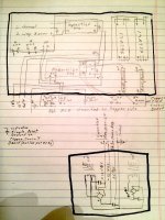
I have attached my hand drawn block diagram showing how I thought this would work right up until I got to the SSLV1.1 regulators driving my Salas phono boards (thank you Salas!).
Now it gets complicated. These regulators have a plus and minus sense wire and how does that effect the grounding for the phono boards?
My original thought was to run every ground to a central point on the copper clad circuit board I am using to hold the RCA input/output jacks. If this looks like it will work please chime in and let me know where the minus sense wire is connected.
The other way to do this is to not ground the ground wire coming into the pre amp, but to run individual ground wires to the regulators, daisy chain the audio board grounds from the regulators and bring the audio board grounds to the RCA copper board central ground.
I haven't committed yet, so I can do it either way. Which way is the least likely to hum?
Looking forward to this long term project's completion, so I can start finishing the power amp projects that are stacking up. F6? I haven't finished the F5 Turbo!
Rush
I have complicated my life with a pre-amp with 3 different regulated power supplies coming from two different transformers.
I have been drilling and fitting and reading and drawing and building and now I come to the fun part (it is all fun) trying to figure out the grounding.
I have attached my hand drawn block diagram showing how I thought this would work right up until I got to the SSLV1.1 regulators driving my Salas phono boards (thank you Salas!).
Now it gets complicated. These regulators have a plus and minus sense wire and how does that effect the grounding for the phono boards?
My original thought was to run every ground to a central point on the copper clad circuit board I am using to hold the RCA input/output jacks. If this looks like it will work please chime in and let me know where the minus sense wire is connected.
The other way to do this is to not ground the ground wire coming into the pre amp, but to run individual ground wires to the regulators, daisy chain the audio board grounds from the regulators and bring the audio board grounds to the RCA copper board central ground.
I haven't committed yet, so I can do it either way. Which way is the least likely to hum?
Looking forward to this long term project's completion, so I can start finishing the power amp projects that are stacking up. F6? I haven't finished the F5 Turbo!
Rush
Attachments
Hello Rush, your PDF presents just a blank page to me at least. Anyway, in general the sense mean to be near where the consumption nodes are. So you should attach your (+) force and sense centrally to where the JFETS nodes draw mA since they all draw about the same in the phono. You should attach the (0) force and sense on the phono board near its last stage's ground node where the signal level is at its strongest. Another thing is its no good widening the loop area between (+) & (0) cables to general GND nodes, it makes them more efficient an antenna. If there will be trafos in same box with the phono, its a hum no-no BTW.
Those were the consumption nodes. Now referencing to general ground is another thing, you may attach GND wires from those same (0) nodes to whatever central point of the whole preamp that does not hum back at you.
P.S. Did you ever present your phono in its thread? I don't recall, was it a success?
Those were the consumption nodes. Now referencing to general ground is another thing, you may attach GND wires from those same (0) nodes to whatever central point of the whole preamp that does not hum back at you.
P.S. Did you ever present your phono in its thread? I don't recall, was it a success?
Hello Rush, your PDF presents just a blank page to me at least. Anyway, in general the sense mean to be near where the consumption nodes are. So you should attach your (+) force and sense centrally to where the JFETS nodes draw mA since they all draw about the same in the phono. You should attach the (0) force and sense on the phono board near its last stage's ground node where the signal level is at its strongest. Another thing is its no good widening the loop area between (+) & (0) cables to general GND nodes, it makes them more efficient an antenna. If there will be trafos in same box with the phono, its a hum no-no BTW.
Those were the consumption nodes. Now referencing to general ground is another thing, you may attach GND wires from those same (0) nodes to whatever central point of the whole preamp that does not hum back at you.
P.S. Did you ever present your phono in its thread? I don't recall, was it a success?
Salas,
I have built your phono and am using your regulators. I haven't fired it up yet. It has been a long project. The transformers are in a separate box.
I took a new jpg photo and enhanced the drawing so you can see my layout.
The crossover is a 4th order using B1 buffers between stages.
I hope the attachment is clearer.
Rush
Attachments
Rush, this system is too complex to predict for best GND scheme. Just remember about the regs that their sense/force scheme targets load consumption close nodes only, as I detailed above. Will be happy to throw some ideas when you will try a likely plan first and can feedback results.
I too will be faced with the same issue in short order. I am drafting and doing the PCB layout for all three BiB regulators needed (+5, -5, -15) for my TDA1541A DAC. True to the Salas design these will be made with the FORCE and SENSE lines. Also on that same PCB will be a pre-regulated 6V supply for the clock and FIFO stage. (A total of 4 regulators)
I also have on a separate PCB the Salas SSHV2 shunt regulator. This will feed the DAC PCB's single tube gain stage plate supply. The question is, where to tie the grounds? I think the sense lines rule out a star-ground topology. With other equipment I have built, as in my power amplifiers, I have always implemented star-point grounding topology with great success.
Any suggestions?
Rush, this system is too complex to predict for best GND scheme. Just remember about the regs that their sense/force scheme targets load consumption close nodes only, as I detailed above. Will be happy to throw some ideas when you will try a likely plan first and can feedback results.
Roger, I don't know about the paculiarities of tying the ground reference of the FIFO buffer and it's own inputs but as far as the 1541A is concerned, it's far better to get the dac chip (a 'plug in' board maybe) close to the power supplies (0, +/-5, -15) (or within a few inches) - having the FIFO's clock as the dac's clock presents it's own difficulties and I would presume that you would need to use the same pin5 gnd point on the 1451A dac chip to ensure best performance/locking but not so sure about adding the FIFO's shunt regs to this point on top - get's to be a matter of sorting out the gnd currents and loops returns.
Most people seem top tie the o/p stage gnd and it's SSHV gnd together and then tie this 'separate' gnd to the same dac's pin 5 gnd point but this depends on if you use a current buffer on the o/p pins of the dac chip complete with it's current source to maintain the o/p pin's 0volts, or an Riv resistor to gnd (as is still often done) and this will firmly tie the front end of the valve gain stage to the dac's pin5.
As you can see, thre are enough areas for ground loop disasters without looking at the far more complicated 'force/sense' wiring.
I thought this was a bit awkward until I had a look at Jeremy's (qusp) computer sourced, ESS dac, with the FIFO, D1 O/P stage, headamp, etc, all with their own supplies! Mucho complicated stuff!
As Stu Yanager said some years ago, a simple good quality transformer with the correct impedance loading can be "Oh So Useful" with some of these designs altho using raw supply isolation can be very effective to avoid transformer current return problems even with the use of the SS regs.
Unfortunately, I can't offer any assistance with the FIFO <-> dac clock and it's not an easy solution with the 1541A as I understand it.
I hope this rambling discourse may be of some use to you ....
You need the 220R or a simple diode in series with the LEDs. You need to jumper the non used positions to close the series Vref circuit. Use a 33R dummy to simulate 150mA load. Set CCS for 200mA minimum. Your now dummy asks for 250mA you are possibly chocking your CCS setting. Find your CCS current by measuring voltage drop across your setting resistor and dividing by its value.
 What is it built for?
Sound better or worst or nothing change?Odac...
- Home
- Amplifiers
- Power Supplies
- SSLV1.1 builds & fairy tales