I will not need a different +ve and -ve version.
I have repeated so many times that the -ve version using only Nchannel devices does both polarity jobs more cheaply and just as well, if not better.
A PCB created for either a +ve version, or a -ve version can very easily be adapted to the other polarity.
I have repeated so many times that the -ve version using only Nchannel devices does both polarity jobs more cheaply and just as well, if not better.
A PCB created for either a +ve version, or a -ve version can very easily be adapted to the other polarity.
Hello,
Some of you may have seen in the Salas Simplistic HV Shunt Reg thread that I have created a small Excel spreadsheet to make calculations of the CCS resistor and MOSFETs dissipations easier.
Well, the BiB already has an excellent build guide, but it was easy enough to modify the HV spreadsheet to make a SSLV1.1 version of the calculator.... so here it is in case it helps someone:
https://docs.google.com/open?id=0B4Rnva0idfhAMmM1ZWM1ODgtOTczYy00M2RmLWI1NDEtYjljZTlhZDIwY2Iy
If you have any question, do not hesitate to ask. Cheers!
Fred
This is the post I tried to link to, I thought I had copied link location in last post as you suggest. The arrow in quote should take you to Post 903.
Lazybutt's spreadsheet is here
http://www.diyaudio.com/forums/power-supplies/192625-sslv1-1-builds-fairytales-19.html#post2861878
No wonder I did not know it existed. It's in Googledocs.
Why did he not attach the doc?
At least it is sorted and now appears in post1.
http://www.diyaudio.com/forums/power-supplies/192625-sslv1-1-builds-fairytales-19.html#post2861878
No wonder I did not know it existed. It's in Googledocs.
Why did he not attach the doc?
At least it is sorted and now appears in post1.
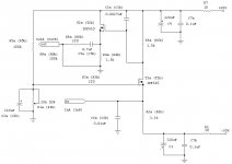
New R103 value of 3.9K, and voltage achieved on the +ve reg. Cheers all for the help.
Congrats and welcome to the BiB club
")
what do you mean when telling digital Vref 220 uF ?
Interesting setup
you are powering only Pass I/V with Salas BIB regulator and everything else with EB serial regulators ? what Is your output voltage fed to Pass I/V what Is your current through CCS ?
CX01-CX02 near the rectangle "SEE TEXT"
Vout +-30V CCS 200mA
If the regulator outputs are located exactly on the amplifier power inputs then the local MF & LF decoupling can be dispensed with.
You can design the two PCBs, PSU & Amplifier, to stack bottom face to bottom face to get as little as 2mm of lead length (a solid copper link) to make best use of very short lead lengths and very low added inductance.
I am not so sure the HF decoupling can be dispensed with, I suspect this is still required across the main output device, i.e. right across the output device, T2a Drain PIN to R4a GND PIN.
C7a is shown in the wrong position on the schematic. C7b may be near useless in it's present location.
Last edited:
- Home
- Amplifiers
- Power Supplies
- SSLV1.1 builds & fairy tales