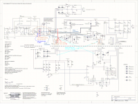
Hi, I need the eyes of an experienced PFC designer... Attached are schematics of the 750W semi-bridgless PFC I'm working on. L4981 controller, toroidal KoolMu boost inductor, CoolMOS transistors, 120VAC input. Series string of 6 100W incandescent bulbs as load. Testing it out w/ a variac, I haven't pushed it past 40% yet.
The diode bridge runs very hot, using a small heatsink, and eventually blew out. My understanding is that this bridge is used to bypass the boost diodes for inrush current during startup, and also to reduce common mode noise by linking the output ground to the AC line. Why is it carrying such current during normal operation? (The output voltage is higher than the peak rectified voltage from this bridge.)
How much capacitance is should I use on the AC-line side of the boost inductor? ST's appnote uses 1uF for an 800W converter, and I started with that value (C23). However, this doesn't attenuate the 50KHz switching noise on the AC line. I added 4.4 uF additional and the switching noise is reduced, but it's still significant. My variac is making a loud audible vibration, likely because of this? Do I need much more?
After removing the bridge temporarily, the fuse blows easily, even at 30% on the variac. Mosfets and diodes are running cool.
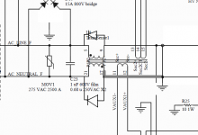
The attached photos include the current-sense voltage measured at the center tap of the current sense transformer L5. It looks as I expect, except that it looks a little distorted for the negative phase of the AC input.
The other photo is the AC line voltage measured before the EMI filter, with a total of 5.4 uF of capacitance across the boost inductor.
(The schematic specifies an ETD59 core, but I substituted two stacked KooMu toroids instead, for a total of 54,000mm^3. The measured value is about 440 uH. D19, D22 were changed to 8V each, rather than 5.1V).
(I'm powering the L4981 with an external supply, since there isn't enough current from the aux winding at 40%.)
Any ideas?
Thanks,
Brian
The diode bridge runs very hot, using a small heatsink, and eventually blew out. My understanding is that this bridge is used to bypass the boost diodes for inrush current during startup, and also to reduce common mode noise by linking the output ground to the AC line. Why is it carrying such current during normal operation? (The output voltage is higher than the peak rectified voltage from this bridge.)
How much capacitance is should I use on the AC-line side of the boost inductor? ST's appnote uses 1uF for an 800W converter, and I started with that value (C23). However, this doesn't attenuate the 50KHz switching noise on the AC line. I added 4.4 uF additional and the switching noise is reduced, but it's still significant. My variac is making a loud audible vibration, likely because of this? Do I need much more?
After removing the bridge temporarily, the fuse blows easily, even at 30% on the variac. Mosfets and diodes are running cool.
The attached photos include the current-sense voltage measured at the center tap of the current sense transformer L5. It looks as I expect, except that it looks a little distorted for the negative phase of the AC input.
The other photo is the AC line voltage measured before the EMI filter, with a total of 5.4 uF of capacitance across the boost inductor.
(The schematic specifies an ETD59 core, but I substituted two stacked KooMu toroids instead, for a total of 54,000mm^3. The measured value is about 440 uH. D19, D22 were changed to 8V each, rather than 5.1V).
(I'm powering the L4981 with an external supply, since there isn't enough current from the aux winding at 40%.)
Any ideas?
Thanks,
Brian
Attachments
Your diode working at high freq spiked voltage, you should use ultrafast and no need that big, and place some snubber if necessary.
Using MKP or equal caps is recommended for that 1uF caps to reduce the spike.
Your PCB layout is very bad. Bad tracing some high current line. Also you placed gate resistor too close to the drain, the other is better, you may look the differences between them at your current graph, and some other bad placed component.
I am not experienced well, and still have some problem with my own PFC too.
Just this what I know.")
Using MKP or equal caps is recommended for that 1uF caps to reduce the spike.
Your PCB layout is very bad. Bad tracing some high current line. Also you placed gate resistor too close to the drain, the other is better, you may look the differences between them at your current graph, and some other bad placed component.
I am not experienced well, and still have some problem with my own PFC too.
Just this what I know.
Hi, thanks for your reply. I noticed that my PDF file wasn't showing the flood-fill on the PCB layout, so I've updated the file. You'll notice that the layout is actually not bad: the high-current loop area is very small, limited by the thickness of the board.
I think I disagree with you about the diode bridge having to use ultrafast diodes. This is not in the high-frequency current path. The top two diodes only conduct during startup, before the boost converter has charged the output caps. The lower two diodes I believe are also outside of the high-frequency path. The MOSFET body diode of the opposite phase conducts the 50KHz current. As a further example, see this semi-bridgeless example, which uses a standard-recovery GBU6J diode bridge. Choosing Between Semi-Bridgeless and Interleaved PFC Pre-Regulators | Jun 2009 Page of
Likewise, ON Semi Appnote AND8392/D uses a 15A 800V slow diode bridge in a semi-bridgeless PFC configuration:
http://www.onsemi.com/pub/Collateral/AND8392-D.PDF
I think something else is going on. Removing this bridge would turn my semi-bridgeless into a normal bridgeless PFC, nothing wrong with that. In this case, why is the current sense still distorted, and why does the fuse blow?
As for the input capacitor, I am using a 1uF Wima MKP, resulting in the waveforms shown. I'll take a closer look at the gate drive at the MOSFETs, but it looked ok when I checked it briefly. The snubbers on gate and drain are currently NOT stuffed, but I do have ferrite beads on the gates.
From that (voltage picture), your diode is working at high spiked place indeed. Placing it before the filter may solve the heating problem, but you will be another EMI problem to the input line. And your PCB layout is very bad, and from that (current picture), there may something disturbing the controller or may be sense faillure.
Lets see to the ON stuff. That PCB has (looks like) three ground plate area, Power stage, controller, and that small converter. You may search any PCB picture that may help you in designing your own.
With blown fuse, just remember that both your mosfet working at coupled transformer/inductor. If there some collision, your fuse will blow, seems this is what happening, from that (current picture) small collision frequently happened.
You need to analyze both gate voltage, and may be drain voltage if necessary.
good luck
Last edited:
Hmm...
Here's an equivalent circuit during the on time. (disregarding rds-on)
L4 is shorted for both input polarities by the lower bridge diodes. It is only the leakage inductance of L4 and circuit resistances that separates this from a hard short across the input. :O
I don't think a coupled inductor will work there either - look at how the input common mode potential changes between the switch on and off states.
Attachments
Last edited:
No, I don't think so. For the positive phase, during the on-time, the top diode you drew is reverse biased. The 50KHz return current flows through the opposite MOSFET body diode, which turns on quickly. The bottom diode you drew is forward biased, but its is slow diode, so it doesn't have time to turn on before the body diode begins conducting.
The lower bridge rectifier diodes only turn on and off at 120 Hz, to keep the output ground referenced to the line's low-side.
See the fig 4 example at http://powerelectronics.com/power_management/805PET23-off-line-power-converter-efficiency.pdf
As for the coupled inductor, see the L4891 appnote Fig 9 and related verbage regarding the use of a coupled inductor rather than two separate inductors. http://www.st.com/stonline/products/literature/an/9119.pdf
Hi koosh,
I found another connector with High voltage line near the sensor wire on P13-P15 connection. Move away that line too.
And that bridge is needed on your circuit, why you remove it? Isn't all will be flying. I've writing about placing this bridge before the filter, it is not work, I am not recognize the function before, when you said that removing it makes your semi-bridgeless into a normal bridgeless PFC.
Also there is no grounding (small grounding caps) from ground to the earth.
Btw why you couple that inductor? Any reference?
Last edited:
Figure 9 in the ST appnote does not have a bridge fitted before the coupled inductor while figure 4 in the other document uses separate inductors. These features are mutually exclusive. No diode, no matter how slow, will be able to stand off the full line voltage, in the forward direction, for the full on-time of the switch without conducting a lot of current. This is what it would have had to do in a circuit with both a coupled inductor and a bridge before the inductor.
But in reality, the coupled inductor solution (without bridge by necessity) is practically unworkable too due to common-mode noise problems. The text regarding common mode noise referring to figure 9 in the ST document is wrong. The common mode rejection is better with separate inductors. Just look at the inductance seen by a common mode current. For coupled inductors it is just the leakage inductance, while it is the inductance of both filter inductors in parallell for non-coupled inductors. The latter will be much higher. It's nowhere near good enough though so that's why you'd want to fit the bridge like in figure 4 you are referring to, which is an approach that will not have extreme common-mode noise problems.
But in reality, the coupled inductor solution (without bridge by necessity) is practically unworkable too due to common-mode noise problems. The text regarding common mode noise referring to figure 9 in the ST document is wrong. The common mode rejection is better with separate inductors. Just look at the inductance seen by a common mode current. For coupled inductors it is just the leakage inductance, while it is the inductance of both filter inductors in parallell for non-coupled inductors. The latter will be much higher. It's nowhere near good enough though so that's why you'd want to fit the bridge like in figure 4 you are referring to, which is an approach that will not have extreme common-mode noise problems.
Last edited:
Eva, megajocke, thanks for your comments. Yes, I see now. That ST appnote misled me. In reality, it's the differential mode signal seeing high impedance (storing energy in the coupled boost inductor), therefore the common mode signal will see a very low impedance. I see how using separate inductors would improve the common-mode attenuation.
I'll have to rebuild my boost inductor into two inductors, each with half the inductance of the existing one.
Do you recommend using 1uF caps connected from the output ground to the AC hot/neutral, in addition to the diode bridge? They provide a high frequency current path between the output and the line, while diodes provide the low-freq path, correct?
If its able to use a coupled, you have bigger core on your inductors. And if there any references it will helpful. May be it need separated gate driving for both mosfet.
Placing only bridge diode will make it heated. Slow diode can't handle high frequency, and your emi transformer may working hard. You need to solve this.
Placing only bridge diode will make it heated. Slow diode can't handle high frequency, and your emi transformer may working hard. You need to solve this.
Are you aware of the special common-mode filter requirements of that topology?
No, sometimes I post my mistakes
don't follow any mistakes.Hi koosh,
Turning off negative side mosfet may solve the collision and that 1uF MKP could be added. It will result in lower vibration between ground and earth. and no need to replace the bridge.
It is interesting ways. I need to try three different PFC in a single transformer sometimes.
Last edited:
Hi, koosh.
Is it replacing only the inductor or overall circuit?
After read more the apnotes, I am now realize that you mixing both semi-bridgeless(with bridge) and bridgeless(with coupled L) in a bridgeless topology.
In this mixture are more difficult to understanding the real current loop path.
The first problem (distortion) is caused by L5 that should not used in semi bridge topology, and actually is not happened (only in sense caused by L5).
The second (blowing fuse) happened when your current loop (through inductor) are become more complex due to high impedance input.
May Eva is right about questioning this, that you need special EMI filtering provide low impedance input (with some LC series to shorten 2 or 3 of the biggest spectrum ripple). If not, there may big current looping in the EMI filter.
Last edited:
Onto Aban: I am replacing the coupled inductor with two separate inductors. However, I think my previous comment about cutting the inductance in half is wrong. Each coil should be the same inductance and the coupled inductor was, since this topology is essentially two separate boost converters, one for each half-cycle.
I realized that my layout had swapped the polarity of L5B, which was the reason the current sense was distorted, causing current spikes on the negative half-cycle.
I believe the current sense transformer L5 is still useable in the semi-bridgeless topology with separate boost inductors. A similar setup is shown in Fig 7 of a TI appnote:
http://focus.ti.com/lit/an/slua517/slua517.pdf
L5b? ..
If by that sense failure, then the driver increasing the pulse width, that causing over current, It should be fine after L5b fixed.
one for each half-cycle? that mean turn off negative side (opposite) mosfet for each half cycle, also replace the driver, and all become semi-bridgeless?
Bridgeless may have best efficiency, but semi-bridgeless have some advantage.
I'll read the appnote.
Hello koosh, although it would thoretically also work with both FETs switching, usually in a bridgeless PFC one FET is kept fully ON during nearly a half cycle (8.33 or 10 ms) while the other one is switching (boosting). I can't see this gate logic in your schem, only your gates paralleled on the L4981. Using the coupled L4 for bridgeless PFC would even be possible, but NOT in combination with the 2 lower diodes of D10 (SHORT!!). Why? There is high AC block voltages across one winding of L4, so it will also appear on the other winding and must not be shorted through series path of lower D10 diode and ON FET (resp. it's body diode). So use 2 coils.
Besides: We have here a 750W bridgeless PFC design (hi and lo line) and I have the following comments: Cool C3 To247 is an already outdated and way overkilled elephant for that power <-> replace by something like IPP60R125C6 (try 15 Ohms on gate) and get faster switching, lower cost and smaller FET design. Invest 2 bucks in good diodes instead: replace slow STTH by ITD05SG60C (sufficient for 750 W, will boost low line efficiency). Special trick: put one AC foil cap in parallel to each of the two lower D10 diodes...
oooh, I think I ve told way too much secrets....
- Status
- This old topic is closed. If you want to reopen this topic, contact a moderator using the "Report Post" button.
- Home
- Amplifiers
- Power Supplies
- Bridgeless PFC help