Hello,
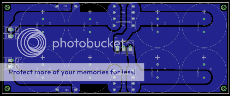
I'm building an F5 amplifier and I am going to try to etch my psu pcb. I just finished the layout and I would like to know if you can see anything wrong with this layout.
I followed the schematic from the owner manual of the F5. I wanted it on one layer as this will be my first try at etching. I know the connectors should be close to the edge, but putting X3 this way was easier... is it gonna be a problem other than aesthetic?
Please go easy on me... this is my first try with eagle.
Thanks !

Yes!
Hi,
Why don't you use two bobble connection in the middle instead of one with three positions? That way you'll have more ground path in the middle instead of a narrow ground in the middle.
Just my two cents.
All the best,
Audiofanatic")
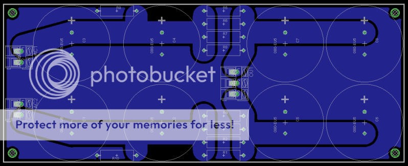
Thanks for this idea Andrew, rotating the 3 way surely improve traces. I also did change the resistors size as thoses I ordered are 15mm and I had first selected 12mm for the layout.
Anything else could improve it?
Thanks !
Hi,
Why don't you use two bobble connection in the middle instead of one with three positions? That way you'll have more ground path in the middle instead of a narrow ground in the middle.
Just my two cents.
All the best,
Audiofanatic
- Status
- This old topic is closed. If you want to reopen this topic, contact a moderator using the "Report Post" button.