I've just finished the pcb design for a regulator I'm developing (see sig). The design is a one layer board. Just when I was about to choose the trace thickness (2oz) it occurred to me that I could make it a two layer board, and have the exact same traces on the top and bottom of the board, thus doubling the effective trace thickness. Then I could use the same board for even higher current.
I can't think of a reason why this shouldn't be done, but I thought I'd ask just in case I'm missing something.
I can't think of a reason why this shouldn't be done, but I thought I'd ask just in case I'm missing something.
Perhaps the layout allows for more criticism.
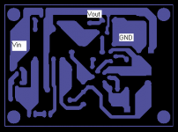
It is the Vin -> Vout trace that could benefit from twice the copper thickness. I was thinking of 3-5A through the regulator. Maybe even more. The shunt mosfet is connected directly to the GND island, as are all the other high current parts. The remote sensing points have a separate connection.
It is the Vin -> Vout trace that could benefit from twice the copper thickness. I was thinking of 3-5A through the regulator. Maybe even more. The shunt mosfet is connected directly to the GND island, as are all the other high current parts. The remote sensing points have a separate connection.
Attachments
IMHO, single layer, short traces, star connection type (where possible) and remote sensing is the correct way.
No need for ground plane, you are not working into RF range. Double layer and ground plane can introduce some capacitance & inductance in unpredictable way. Big ground plane for few connection points across that plane + remote sensing wires returning to ground plane at some point = ground loop
No need for ground plane, you are not working into RF range. Double layer and ground plane can introduce some capacitance & inductance in unpredictable way. Big ground plane for few connection points across that plane + remote sensing wires returning to ground plane at some point = ground loop
- Status
- This old topic is closed. If you want to reopen this topic, contact a moderator using the "Report Post" button.