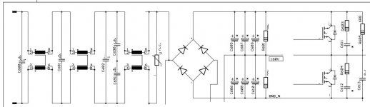
It it OK to split the
Filter Stage, Bridge, The 2200uf/200V capacitors/Delay ON circuit to a separate board?
AND to take the + 0 - 360V through a cable to the switching board that CONTAINS.
IGBT, ETD59, Output Diodes, Driver SG3525, Output Capacitors, Current Limit, Short Circuit protection.
I don't know if it OK to do that!
Please advice.
The input capacitors, switching stage with drivers, transformer, output rectifiers, output inductors (if any) and output capacitors should be together because high frequency high currents are flowing on these paths and parasitic inductance matters a lot.
The control circuit may be in another PCB as long as signals are interfaced properly.
Input EMI filter, input rectifiers and softstart may be in another PCB too, or even point to point (for early prototypes), as only low frequency currents flow there.
If you are not experienced, start to visualize things in terms of parasitic inductances and capacitances that form LC resonators. For example, the inductance of the 2200u 200V capacitors in series, together with the inductance of the leads of the IGBT package and PCB tracks, will resonate with the internal C-E capacitance of the IGBT that is turned off, typically between 10 and 50Mhz. Parasitic winding capacitance and the inductance of the connections to that capacitance may also add resonant modes.
These resonances work like the strings of a guitar, they are plucked on each switching event and will keep singing (and producing EMI) for a certain time if proper damping is not included. The higher the parasitic inductances and capacitances, the more energy will have to be dissipated in the damper snubbers.
Wires are highly inductive and very good EMI radiating antennas (in comparison to a PCB with ground plane) so they have to be avoided completely in high frequency paths.
Last edited:
OK
Thank you EVA,
but your answer is complex for me to understand, since I am not that expert in SMPS.
Therefor you recommend to put all the stuff on one PCB? that will be large!
Regarding the ground plan, it should be connected to witch ground? OUTPUT or INPUT?
That circuit will operate at 125KHZ, what power do I expect from that frequency with ETD59
Can I get 1.7KW Continues?
SEE CAPACITOR, LINE FILTER
Thank you
Last edited:
Suggeset?
Hi EVA.
What do you suggest?
I already have all values for all components.
and I am sticking to the schematic, and parts values.
The only thing I dont know is the output Transformer, witch I will use ETD59. with LITZ Wire
In my previous project, I had dozen of blown MOSFETS in that design. I dont know how to prevent that!
Please your advice.
Thank you EVA
I think you are trying to go to fast. If you make a prototype without understanding how parasitic Ls and Cs work, many unexpected failures and dozens of blown IGBT/MOSFET are likely to be the result.
Hi EVA.
What do you suggest?
I already have all values for all components.
and I am sticking to the schematic, and parts values.
The only thing I dont know is the output Transformer, witch I will use ETD59. with LITZ Wire
In my previous project, I had dozen of blown MOSFETS in that design. I dont know how to prevent that!
Please your advice.
Thank you EVA
Last edited:
Hi Microsim,
I'd say that splitting just before the rectifier would be wise, and in fact, it's good practice to keep the line filter isolated (shielded if possible) from the main supply to prevent injecting radiated noise back into the line after the filter.
The bulk capacitors after the rectifier need to be close to the IGBT's. Local decoupling is also a good idea. As Eva said, you need to carefully consider HF return paths.
As for the ETD49, you should have no problem getting 1700W a that frequency if it's designed correctly. If it's running at full power all the time, you'll probably need active cooling, and you'll have to balance out your core and copper losses in the transformer.
On another note, Eva is absolutely correct - you seem to be going a little too fast. Getting a supply like this to work and not pollute the entire house with EMI is not a trivial matter. Even with a full set of design skills, a fully functional supply, and an EMI lab, it's still a struggle to optimize for low EMI and meet standards. Without all of the above, you don't stand a chance. It's just the nature of high power switch-mode electronics.
I would suggest looking into a lower power project, and maybe using an integrated solution like the parts from Power Integrations. They make small integrated controllers/fets called Topswitch. You can use their software to design what you need (up to 300W I think) and at least that way you can get some experience with the other aspects of SMPS (transformer, line filter etc...) without taking on everything at once.
Best of luck!
Owen
Hello.
I think that all of are right, BUT you are talking too professional also.
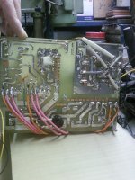
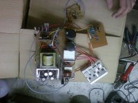
In my previous SMPS, (See Pictures) its not that professional, but that was my second project after building the K6 SMPS from (A&T LAB) That supply are crap any way, it failed.
The second one I built was better, I got +-80V 7.4 AMPERE. with good ventilation. I Tried it with power amplifier, things was very good ( I BLOWN UP MANY MOSFETS) i cannot deny that but DUE MY Mistakes.
In this new design I will try to eliminate those things with your help all !
See pictures
I think that all of are right, BUT you are talking too professional also.
In my previous SMPS, (See Pictures) its not that professional, but that was my second project after building the K6 SMPS from (A&T LAB) That supply are crap any way, it failed.
The second one I built was better, I got +-80V 7.4 AMPERE. with good ventilation. I Tried it with power amplifier, things was very good ( I BLOWN UP MANY MOSFETS) i cannot deny that but DUE MY Mistakes.
In this new design I will try to eliminate those things with your help all !
See pictures
Attachments
Microsim:
I'm a little worried now... the Y-caps need to go to chassis, and I don't see any 6mm isolation on that PCB. This is basic safety, and needs to be followed. Those caps also need to be rated appropriately. The exclamation mark and triangle are on the schematic for a reason.
If you're not familiar with basic off-the-line switcher safety, I would strongly suggest you read up on it, and strongly suggest you not attempt any project that is beyond your abilities in the safety department.
If it ever caught fire and burned your house down, your insurance company would laugh in your face and you wouldn't get a dime. At least if you can prove due diligence you might stand a chance.
Also, you'll probably have problems with light-load stability with a very high power SMPS hooked up to a class AB amp with light bias.
Cheers,
Owen
Microsim:
I'm a little worried now... the Y-caps need to go to chassis, and I don't see any 6mm isolation on that PCB. This is basic safety, and needs to be followed. Those caps also need to be rated appropriately. The exclamation mark and triangle are on the schematic for a reason.
If you're not familiar with basic off-the-line switcher safety, I would strongly suggest you read up on it, and strongly suggest you not attempt any project that is beyond your abilities in the safety department.
If it ever caught fire and burned your house down, your insurance company would laugh in your face and you wouldn't get a dime. At least if you can prove due diligence you might stand a chance.
Also, you'll probably have problems with light-load stability with a very high power SMPS hooked up to a class AB amp with light bias.
Cheers,
Owen
ok. you are right, and those are the notes i want to hear
as i know the 6mm clearance is required in the other board, not the EMI stage!
the capacitors you cant see, are added in the last pcb. and can i use the ground plan on the pcb as the chassis?
And regarding safety, I know exactly what I am doing, and I have serious protection methods before the test will began
Also I have just knew a French engineer who offered me FREE support for this project, and will assemble this supply together, since he is a SMPS engineer with 4 years experience.
So he will check every thing before that late stage ( the testing)
Also I had no problems with my previous prototype of SMPS with light-load stability, that was 900W +-100V, with the 1000W load dropped to +-82V what I mean, the voltage almost the same, but higher current!!
since no one in here offered free support for this project!

Last edited:
What consequences do you expect from having the switching transistors connected to the PCB with 15cm long wires that don't even run close one to another?
In the reply to this question is the solution to your problem
In my first off-line SMPS prototype 10 years ago I didn't even use a PCB, all was point to point and waveforms were terrible, but it could do 15V 120A regulated output. Parasitics were making things fail and that thing was capable of disturbing a CD player that was on the same room.
This may sound like a joke but now I have the opposite problem with the last revision PCBs of the class D amplifier in which I'm working: Too low parasitic inductances. During body diode reverse recovery, current slope (di/dt) depends on gate supply voltage, gate turn-on resistor and parasitic source path inductance (somebody understanding that would never use wires). The latter has become so low that it's difficult to achieve a safely low di/dt without compromises in the first two factors. Origilally MOSFET were failing at high current and high temperature because the layout was handling over 1500A/us per body diode without problem. Then I noticed that parasitic inductances were less than half of what I was expecting
Concerning the insulation practices, In the beginning I learned a lot by studying commercial SMPS of various kinds and its transformers. Much later I had access to the papers describine standards (quite dense), but I alwas understood intuitively why everybody was leaving 5 to 10mm spacing between primary and secondary side on the PCBs and margins on the transformers Sometimes I was feeling that layouts and semiconductor choices were leaving some room for improvement, but a good layout or good efficiency are not required for certifications, proper insulation is.
In the reply to this question is the solution to your problem
In my first off-line SMPS prototype 10 years ago I didn't even use a PCB, all was point to point and waveforms were terrible, but it could do 15V 120A regulated output. Parasitics were making things fail and that thing was capable of disturbing a CD player that was on the same room.
This may sound like a joke but now I have the opposite problem with the last revision PCBs of the class D amplifier in which I'm working: Too low parasitic inductances. During body diode reverse recovery, current slope (di/dt) depends on gate supply voltage, gate turn-on resistor and parasitic source path inductance (somebody understanding that would never use wires). The latter has become so low that it's difficult to achieve a safely low di/dt without compromises in the first two factors. Origilally MOSFET were failing at high current and high temperature because the layout was handling over 1500A/us per body diode without problem. Then I noticed that parasitic inductances were less than half of what I was expecting
Concerning the insulation practices, In the beginning I learned a lot by studying commercial SMPS of various kinds and its transformers. Much later I had access to the papers describine standards (quite dense), but I alwas understood intuitively why everybody was leaving 5 to 10mm spacing between primary and secondary side on the PCBs and margins on the transformers
Sometimes I was feeling that layouts and semiconductor choices were leaving some room for improvement, but a good layout or good efficiency are not required for certifications, proper insulation is.
Last edited:
Eva
Hi EVA,
Those wires are totally wrong, but in that design there was no enough space for the heat sink, AND that supply worked,(almost).
Test was on halogen lamp 1000W for 1 Hour with FAN. I don't know, worked.
But mosfets used to blow fast at 1000W load, at 700W worked for 5 hours!!
I understand that SMPS is not an easy project, but I need more information's to prevent too many errors.
Thank You
- Status
- This old topic is closed. If you want to reopen this topic, contact a moderator using the "Report Post" button.
- Home
- Amplifiers
- Power Supplies
- SMPS EMI Stage