Hi maxpou,
What kind of material is it? Amplifier?
Eric
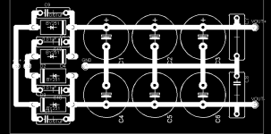
maxpou said:I would like to know where is the best place for output voltage in my PS layout...
What kind of material is it? Amplifier?
Eric
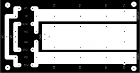
One thing about the layout is that the traces could be wider to reduce resistances.
Remember: It does not cost any extra to widen traces on PCBs. On the contrary, removing copper uses up the solvent used to dissolve it. When working with low frequency power circuits (where stray capacitance is unimportant), a good way to think of this is to start with a layout of all copper, then remove strips just wide enough to ensure enough clearance between nodes. Which is really what you're doing when making a PCB.
Remember: It does not cost any extra to widen traces on PCBs. On the contrary, removing copper uses up the solvent used to dissolve it. When working with low frequency power circuits (where stray capacitance is unimportant), a good way to think of this is to start with a layout of all copper, then remove strips just wide enough to ensure enough clearance between nodes. Which is really what you're doing when making a PCB.
Re: Re: best place for output voltage
Salut Éric,
no it's for my shunt reg for my line stage. Why? Maxpou
Eric Juaneda said:Hi maxpou,
What kind of material is it? Amplifier?
Eric
Salut Éric,
no it's for my shunt reg for my line stage. Why? Maxpou
star882 said:One thing about the layout is that the traces could be wider to reduce resistances.
Remember: It does not cost any extra to widen traces on PCBs. On the contrary, removing copper uses up the solvent used to dissolve it. When working with low frequency power circuits (where stray capacitance is unimportant), a good way to think of this is to start with a layout of all copper, then remove strips just wide enough to ensure enough clearance between nodes. Which is really what you're doing when making a PCB.
Hi Star882,
i post my PCB with bigger trace, but i don't how to start with a layout of all copper and remove strips. i use eagle as software. Maybe you can explain to me. Thank you! Maxpou
Attachments
For the same reason that it's good to take the output voltage from where you have it now, it is also a good idea to make a star ground point at the same end, between the two voltage outputs. All ground connections should be made there, except the transformer centre tap connections, which should be kept at the other end, near the bridge where you have "GND" written already.
That's good. The idea is that since you already paid for the copper, you might as well use it to reduce stray resistance.maxpou said:
Hi Star882,
i post my PCB with bigger trace, but i don't how to start with a layout of all copper and remove strips. i use eagle as software. Maybe you can explain to me. Thank you! Maxpou
...er, I think you can obtain this result in Eagle still by drawing the traces (i.e. not doing the "negative" drawing).
It's just that you draw the traces "thick enough".
For not-very-complex circuits (typically power supply like yours)
I have sometimes tried to paint all the copper of the PCB with varnish, and then scratch it off from the parts to remove (duh!) just like suggested.
The ideal type of varnish is the ground they use for "etching" and printing in fine arts (sorry, don't know the exact English term - aquatint?). This type of varnish remains easy to "etch/scratch" with a needle (screwdriver, actually) and doesn't "chip", it's kind of waxy.
But this process becomes tedious if you need to be very precise (like for ICs).
_
- Status
- This old topic is closed. If you want to reopen this topic, contact a moderator using the "Report Post" button.
- Home
- Amplifiers
- Power Supplies
- best place for output voltage