Yes, That's three times in as many days. I going to book myself in!
Do not even think about that Andrew.... We would all loose a crucial source of knowledge.

You can be sure your writings are read and apreciated.
Not only by me but by most readers that follow your posts for a long time.
We lear a lot from you.
Ditto!!!
+3You can be sure your writings are read and apreciated.
Not only by me but by most readers that follow your posts for a long time.
We lear a lot from you.
Picture a BJT instead of a MOSFET and its nothing more than the classic ''ring of two'' CCS concept.
http://www.diyaudio.com/forums/tube...wo-ccs-differential-triode-amp-stability.html
Sorry for the delay, I was hit by work as my vacation ended. Now recovering from a bike accident I can get some fun done
")
Regarding the circuit, I was under the impression that Id is dependent on Vgs AND Vds. Looking at the 9610 datasheet I can see that, for -Vds > some 100mV, Id is practically constant given Vgs.
Then it's easy
If Vin increases, initially nothing happens in the FET part. The BJT will have to see an increased Ic - if Vce is constant (=Vgs) then Ic = (Vin - Vce) / (R2 + R3).
In order to increase Ic, Vbe must increase. But here we have exponential dependency so even the slightest increase in Vbe will make Ic increase. Because of this, the circuit is almost independent on Vin.
And one simple obvious way to improve this is to replace R2+R3 with a CCS, then Ic and also Vbe will be constant; the increased voltage drop given increase in Vin will happen over this CCS.
Thanks
And there can only be one explanation to the strange behaviour I see: instability - even if it does not show up anywhere.
Also, while looking at the 9610 datasheet I must admit, this FET has possibly only one advantage: it's cheap...
Next prototype will probably be 9240 based (got some in my stash now) and with the BJT/FET CCS with R2+R3 (R4 + R10 in the original) replaced with a K170.
Last edited:
Even cheaper are the N channel. They perform a bit better. Less capacitance, more transconductance.
Noted, thanks
A -ve Salas regulator can be used for a +ve supply.
Something similar to attached, I guess...
Attachments
The worst case dissipation for Q1 is highest mains voltage and output shorted.
The worst case dissipation for Q4 is open output. Main voltage has no effect until after Q1 has failed.
Q1 will always have a worst case dissipation that is >> worst case for Q4.
However, although Pmax should indicate using a high dissipation device for Q1, the consensus coming from the sims, seems to be to use a smaller device for Q1 for best performance.
Be careful to ensure CCS1 can stand worst case mains voltage (add a resistor location to the PCB). This location can use a cascode device or another voltage dropping component.
Also, look after Vbe Q3, due to zero volts across C2 at start up.
Last edited:
...
However, although Pmax should indicate using a high dissipation device for Q1, the consensus coming from the sims, seems to be to use a smaller device for Q1 for best performance.
...which is probably because worstcase Pmax for Q1 and Q4 are much different from "normal operation" (and, btw, does never happen at the same time
).In my case: 25V in, 18V out, 100mA idle/max out:
a) No load:
Pq1 = (25V-18V) x 0.1A = 0.7W
Pq4 = 18V x 0.1A = 1.8W
b) Assuming full load (100mA):
Pq1 = same = 0.7W
Pq4 = 18V x 0A = 0W
c) Worst case:
Pmax,q1 = 27.5V x 0.1A = 2.75W (output shorted, +10% mains)
Pmax,q4 = 18V x 0.1A = 1.8W (no load)
Normally the circuit operates between a) and b) where Pq1 is practically constant and Pq4 diminishes with increased load.
Last edited:
Why is base stopper needed for BC550? It will not increase regulator output noise?
Some schematics shows 1ohm for that position (this will not add to much to rb and hence noise), other 47 ohms. What is the correct value? There are stability issues without this resistor?
Some schematics shows 1ohm for that position (this will not add to much to rb and hence noise), other 47 ohms. What is the correct value? There are stability issues without this resistor?
They are part of the OLG PM and curve shaping. In those schematics that they are minimal value their position is there to have option for shaping the OLG if using different Mosfet types. Which one you refer to? 1.1 has minimal value there for instance.
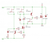
BiB with IRF9610 for CCS and IRF9530?
Use 1 Ohm or zero Ohm link for that as designated in its BOM. Its config works nicely without any higher stopper value which I avoided since its wide bandwidth enough to be more affected for noise. The Vref shunt cap's filter value is noise critical and you can go to 1000uF for good 1/F if its required.
Use 1 Ohm or zero Ohm link for that as designated in its BOM. Its config works nicely without any higher stopper value which I avoided since its wide bandwidth enough to be more affected for noise. The Vref shunt cap's filter value is noise critical and you can go to 1000uF for good 1/F if its required.
Well ... the problem is that BiB for 15V out with WIMA 10uF MKS + 1ohm for snubber and 0.1uF as decoupling capacitor is not starting well without putting the finger on the back of circuit, around output mosfet
The behavior is strange and the output voltage is not stable right after startup. It seems that is on verge of oscillations.
It starts well if 0.1ohm resistor is inserted in series at the input of the circuit which BiB is powering
- Status
- This old topic is closed. If you want to reopen this topic, contact a moderator using the "Report Post" button.
- Home
- Amplifiers
- Power Supplies
- The simplistic Salas low voltage shunt regulator