SSHV2
Here is SSHV2. Same parts count as SSHV, same concept. I put it first in the picture in mid summer. My goals were: 1. More resolution but unchanged musical tone from previous version. 2. Better voltage stability. 3. Adjustable constant current setting on the fly.
I was content at a point, but I wanted to know if users of the popular previous SSHV will find it truly easy and better. So I kindly asked two members to give it a go on their own construction approach, no specific build guide. That was to check if its technique & layout tolerant and how they would like it on different applications. Incidentally both live in Mediterranean islands. First guy runs it for over a month now, had made various builds. Second guy is about to finish his first. They will give you their feedback eventually I believe.
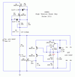
As you can see its cascoded both for CCS and error amp. That is to increase CCS performance and error amp's current/thermal stability. The Q1,Q2 Supertex DN2540 DMOS CCS runs only Q2's Vgs across R4 trimmer that can take the low dissipation, also aided by R3. Because each DMOS has own IDSS just like a JFET, the trimmer not only homes in to the current we need to set, but saves calculations, and of course can be changed at will when the circuit is live. R5 is a safe break and test point. Setting 40mA CCS should read 0.4V across R5 T.P. for instance. R1,R2 gate stoppers should be closest to gates, D1, D2 are Zener protections.
The error amp Q4,Q5 is built around superior PNP Sanyo FBET types (cheaply available as Fairchild) and runs 3 times the current of previous SSHV. Due to voltage sharing across the cascode, current is better SOA tolerated and drives Q3 Enhancement mode MOSFET's input capacitance stronger in high frequency. For easy sourcing reasons, MJE350 has been tested compatible too. Up to 300V that was, without mini sinks on Q4, Q5. Mini sinks are recommended for higher Vout or when in hot enough surroundings. Good for long term reliability anyway.
The Vref is based on Q6 Toshiba 2SK117GR low noise, that showed better drift than previous due to different output conductance and D4 LED's counter thermal coefficient action to Q5's Vbe. R11 trimmer sets Vout, and is R12 ''bypassed'''. C2 noise filtering has been increased to big enough practical MKP size, D3 protects the Vref along initial slower charging time than before. Zobel termination has been adjusted to the now total ''faster'' reg. C1 is MKP too. Both capacitors quality is thought subjectively influential.
Due to the cascode CCS better HF PSRR a 47uF MKP capacitor can be enough for the raw DC, especially if CLC filtered, so to have a chemical capacitors free PSU.
Due to the speedier circuit, 4 wire remote sensing output has been judged useful to be incorporated. It got tested with such output only, without problems. In tube builds that things tend to be lengthier for wiring due to the heat and size of big active components, R.S. can make a perceivable difference. The 4 wires can be shorted right at the reg's output of course if it has to drop in an existing two wire run. I.e. S+ & F+ be turned to one +Vout node, as S0 & F0 to one ground node also.
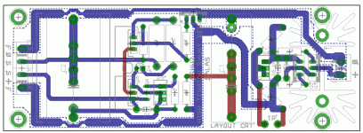
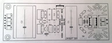
To be thorough I had even consulted a double layer PCB layout with Crt. You can follow it as a general orientation example to put together your own build. Perforated board works fine also and the circuit is same parts count as before.
SSHV2 is conservatively rated as 400V input & 380V output. 20V drop over it is more than enough to regulate well, hence the smaller on board CCS sink. Calculate/test that your transformer and rectification provides at least 10V raw DC more than your Vout goal when your mains are at their worse low. Most of dissipation happens on output MOSFET and is Vout*(CCScurrent-Loadcurrent) in Watt, exactly as you know from previous versions. That will take a main external side/parallel sink of course. If your raw DC in is large for some existing trafo reason check the drop over Q1 ~(Vin-Vout) times the CCS current, maybe you want to add Q1 on main sink too. Well, that's all folks.")
*Short guide added on Feb 2012 after a successful prototypes test run. Small changes in trimmer values and 2 resistors values. Minor update on pcb labeling and guide on May 2015.
** SSHV2 Group Buy thread
Here is SSHV2. Same parts count as SSHV, same concept. I put it first in the picture in mid summer. My goals were: 1. More resolution but unchanged musical tone from previous version. 2. Better voltage stability. 3. Adjustable constant current setting on the fly.
I was content at a point, but I wanted to know if users of the popular previous SSHV will find it truly easy and better. So I kindly asked two members to give it a go on their own construction approach, no specific build guide. That was to check if its technique & layout tolerant and how they would like it on different applications. Incidentally both live in Mediterranean islands. First guy runs it for over a month now, had made various builds. Second guy is about to finish his first. They will give you their feedback eventually I believe.
As you can see its cascoded both for CCS and error amp. That is to increase CCS performance and error amp's current/thermal stability. The Q1,Q2 Supertex DN2540 DMOS CCS runs only Q2's Vgs across R4 trimmer that can take the low dissipation, also aided by R3. Because each DMOS has own IDSS just like a JFET, the trimmer not only homes in to the current we need to set, but saves calculations, and of course can be changed at will when the circuit is live. R5 is a safe break and test point. Setting 40mA CCS should read 0.4V across R5 T.P. for instance. R1,R2 gate stoppers should be closest to gates, D1, D2 are Zener protections.
The error amp Q4,Q5 is built around superior PNP Sanyo FBET types (cheaply available as Fairchild) and runs 3 times the current of previous SSHV. Due to voltage sharing across the cascode, current is better SOA tolerated and drives Q3 Enhancement mode MOSFET's input capacitance stronger in high frequency. For easy sourcing reasons, MJE350 has been tested compatible too. Up to 300V that was, without mini sinks on Q4, Q5. Mini sinks are recommended for higher Vout or when in hot enough surroundings. Good for long term reliability anyway.
The Vref is based on Q6 Toshiba 2SK117GR low noise, that showed better drift than previous due to different output conductance and D4 LED's counter thermal coefficient action to Q5's Vbe. R11 trimmer sets Vout, and is R12 ''bypassed'''. C2 noise filtering has been increased to big enough practical MKP size, D3 protects the Vref along initial slower charging time than before. Zobel termination has been adjusted to the now total ''faster'' reg. C1 is MKP too. Both capacitors quality is thought subjectively influential.
Due to the cascode CCS better HF PSRR a 47uF MKP capacitor can be enough for the raw DC, especially if CLC filtered, so to have a chemical capacitors free PSU.
Due to the speedier circuit, 4 wire remote sensing output has been judged useful to be incorporated. It got tested with such output only, without problems. In tube builds that things tend to be lengthier for wiring due to the heat and size of big active components, R.S. can make a perceivable difference. The 4 wires can be shorted right at the reg's output of course if it has to drop in an existing two wire run. I.e. S+ & F+ be turned to one +Vout node, as S0 & F0 to one ground node also.
To be thorough I had even consulted a double layer PCB layout with Crt. You can follow it as a general orientation example to put together your own build. Perforated board works fine also and the circuit is same parts count as before.
SSHV2 is conservatively rated as 400V input & 380V output. 20V drop over it is more than enough to regulate well, hence the smaller on board CCS sink. Calculate/test that your transformer and rectification provides at least 10V raw DC more than your Vout goal when your mains are at their worse low. Most of dissipation happens on output MOSFET and is Vout*(CCScurrent-Loadcurrent) in Watt, exactly as you know from previous versions. That will take a main external side/parallel sink of course. If your raw DC in is large for some existing trafo reason check the drop over Q1 ~(Vin-Vout) times the CCS current, maybe you want to add Q1 on main sink too. Well, that's all folks.
*Short guide added on Feb 2012 after a successful prototypes test run. Small changes in trimmer values and 2 resistors values. Minor update on pcb labeling and guide on May 2015.
** SSHV2 Group Buy thread
Attachments
Add 100r or something in series with vr4
Swap values of vr11 & r12, 1kvr & 510r
The total dissipation of r9+r10 cannot exceed 1W for <=380Vdc output.
I agree that applying 25% to the power rating is good for reducing temperature drift. But does R10 need to be quite so high in value. What about adding a large value resistor in parallel? Maybe 220k?
VR4//R3 takes it in test and can be substituted for a resistor too in a finalized build. For long term wiper health security, especially if someone wants more than 50mA. If with 100R in series to share more dissipation, it unfortunately closes the CCS much lower than IDSS capability. R9 & R10 along VR11//R12 values work well with 4mA mid point K117GR in my stash for noted Vo range. Plus the higher, the better they get filtered by C2, and the stabler as you mentioned. VR11 suffers no appreciable current. If someone has 1K trimmer already can swap the VR11/R12 values, no problem.
VR4//R3
What happens if the VR is set to 0r1?
What happens if a protection resistor of suitable value is added in series with VR4?
R12//VR11
The temp coeff of the VR is usually much wider than a fixed resistor. Swapping the values improves the overall temp coeff.
R10//220k (or other appropriate value)
Reducing the effective resistance of 68k down to ~52k. Resulting in the CR being reduced by XY%
The reduction in Vce of Q5 is a larger % and this results in less temperature change of the BJT, with the slight improvement of temp coeff.
If CR is critical then increase both R9 & R10 to 75k or 82k or ...
I would prefer that Q5:Q4 Vce ratio be << 1:1
What about 1:4. That would require a higher voltage, Vce0, part for Q4 if high output voltage is needed.
Using three 47k in series for R10=47k and R9=94k gives the benefit of reducing the dissipation in these resistors and increasing the Cr for ripple reduction and reduces temp coeff of the resistors and reduces the temp coeff of Q5.
But then Q4 must be changed for a higher Vce0. All this for 1 extra resistor PCB area.
Last edited:
What happens when VR4=0R is 10R R5 sees all Q2's Vgs. ~2.5V in average DN2540. VR4 dissipates nothing, R3 ~ 0.25W max for most DN2540. That is a border setting, most use these shunts for 50mA-60mA max as seen in this thread. VR4 has 0.5W spec in Bourns shared with R3 and partly R4 in mid position.
I prefer R12 gets the most current in lower Vo set range, but in practice the JFET for ambient temp is much more sensitive to render other small considerations secondary.
I prefer R12 gets the most current in lower Vo set range, but in practice the JFET for ambient temp is much more sensitive to render other small considerations secondary.
Here is SSHV2. Same parts count as SSHV, same concept. I put it first in the picture in mid summer. My goals were: 1. More resolution but unchanged musical tone from previous version. 2. Better voltage stability. 3. Adjustable constant current setting on the fly.
I was content at a point, but I wanted to know if users of the popular previous SSHV will find it truly easy and better. So I kindly asked two members to give it a go on their own construction approach, no specific build guide. That was to check if its technique & layout tolerant and how they would like it on different applications. Incidentally both live in Mediterranean islands. First guy runs it for over a month now, had made various builds. Second guy is about to finish his first. They will give you their feedback eventually I believe.
As you can see its cascoded both for CCS and error amp. That is to increase CCS performance and error amp's current/thermal stability. The Q1,Q2 Supertex DN2540 DMOS CCS runs only Q2's Vgs across R4 trimmer that can take the low dissipation, also aided by R3. Because each DMOS has own IDSS just like a JFET, the trimmer not only homes in to the current we need to set, but saves calculations, and of course can be changed at will when the circuit is live. R5 is a safe break and test point. Setting 40mA CCS should read 0.4V across R5 T.P. for instance. R1,R2 gate stoppers should be closest to gates, D1, D2 are Zener protections.
The error amp Q4,Q5 is based around superior PNP Sanyo FBET types (cheaply available as Fairchild) and runs 3 times the current of previous SSHV. Due to voltage sharing across the cascode, current is better SOA tolerated and drives Q3 Enhancement mode MOSFET's input capacitance stronger in high frequency. For easy sourcing reasons, MJE350 has been tested compatible too. Up to 300V that was, without mini sinks on Q4, Q5. Mini sinks are recommended for higher Vout or when in hot enough surroundings. Good for long term reliability anyway.
The Vref is based on Q6 Toshiba 2SK117GR low noise, that showed better drift than previous due to different output conductance and D4 LED's counter thermal coefficient action to Q5's Vbe. R11 trimmer sets Vout, and is R12 ''bypassed'''. C2 noise filtering has been increased to big enough practical MKP size, D3 protects the Vref along initial slower charging time than before. Zobel termination has been adjusted to the now total ''faster'' reg. C1 is MKP too. Both capacitors quality is thought subjectively influential.
Due to the cascode CCS better HF PSRR a 47uF MKP capacitor can be enough for the raw DC, especially if CLC filtered, so to have a chemical capacitors free PSU.
Due to the speedier circuit, 4 wire remote sensing output has been judged useful to be incorporated. It got tested with such output only, without problems. In tube builds that things tend to be lengthier for wiring due to heat and size of active components, R.S. can make a perceivable difference. The 4 wires can be shorted right at the reg's output of course if it has to drop in an existing two wire run. I.e. S+ & F+ be turned to one +Vout node, as S0 & F0 to one ground node also.
To be thorough I had even consulted a double layer PCB layout with Crt. You can follow it as a general orientation example to put together your own build. Perforated board works fine also and the circuit is same parts count as before.
SSHV2 is conservatively rated as 400V input & 380V output. 20V drop over it is more than enough to regulate well, hence the smaller on board CCS sink. Calculate/test that your transformer and rectification provides at least 10V raw DC more than your Vout goal when your mains are at their worse low. Most of dissipation happens on output MOSFET and is Vout*(CCScurrent-Loadcurrent) in Watt, exactly as you know from previous versions. That will take a main external side/parallel sink of course. If your raw DC in is large for some existing trafo reason check the drop over Q1 ~(Vin-Vout) times the CCS current, maybe you want to add Q1 on main sink too. Well, that's all folks.
Congratulations Nick
, do you know if will be a GB for the new PCB?Congratulations Nick
I must first know that people tried, liked, want, then I can organize something. Its a new thing. Make one p2p and let us know your opinion VS previous if you fancy. You are an SSHV user, so can compare/feedback seriously.
This explains that R5 is the protection resistor.What happens when VR4=0R is 10R R5 sees all Q2's Vgs. ~2.5V in average DN2540. VR4 dissipates nothing, R3 ~ 0.25W max for most DN2540. That is a border setting, most use these shunts for 50mA-60mA max as seen in this thread. VR4 has 0.5W spec in Bourns shared with R3 and partly R4 in mid position.
Why put R5 outside the VR adjustment loop? Put it in series with VR4.
Its as is to be a fixed current calc test point too. If in loop it will be //. I am content generally to as it is now, I appreciate all ideas, but lets wait for independent feedback to see if there are setting or performance difficulties on 3rd party hands so to focus addressing such beyond tampering so early. Thanks.
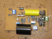
Thanks for including the layout, no need to wait for PCB's. I've been driving a WE417A at 18 ma single feed OTP to very sensitive grados for at least a year with the old SSHV. Thing is noiseless, noisefloor is below -100dB except for a small pump at 60hz mostly from the OPT's picking stray interferance. Possibly do have an oscillation issue at higher power levels but I pretty sure that was from the WE417 not the SSHV. IMD is higher than I would like but the sound is great.
Been waiting on this update, planning on a DHT running more current(~35 ma) and using CCS + parrafeed this time. If using a CCS I would imagine that would mitigate any of the issues around driving an inductive load at higher currents ?
Been waiting on this update, planning on a DHT running more current(~35 ma) and using CCS + parrafeed this time. If using a CCS I would imagine that would mitigate any of the issues around driving an inductive load at higher currents ?
Salas sent me the new schematic some time ago and told me if I had time to test his new circuit. He knew I am using a 26 pre, so I needed around vin 180 and vout 140v out from the regulator. I jumped on it and finished it the next day. Initially I did not give much attention to layout, but it worked right away. I liked that I could adjust current on the fly. During testing it seemed much more stable than SSHV1. Voltage drift was only a few volts after warm up, and then it stays were you adjust it.
I tested it with mje350 initially and it worked fine. When later got the ksa1381 no problems again. Also made a version with vin 330v and vout 300v just to see that there is no problem with it.
Comparing with the first SSHV sound is much better. More definition and more liquid sound I could say. Initial impression was that I got more information on the bass region. Also changing to ksa1381 made a difference.
I attach a picture of my final built. When Salas told me I could do better on the layout, I dismantled both shunts (yes, I built two initially) and rebuilt them!
Attachments
Last edited:
I forgot to mention that my 26 pre has ll1660pp output transformers and SSHV2 is feeding them. There is absolutely no noise or anything on 100db speakers. I really think that this is a worthwhile upgrade from SSHV1 on reliability, ease of construction and especially sound.
Also when tested at more than 300v the ksa1381 were not getting very warm. I do not thin that they need any sinking, but that could change if in a box. But then it' s easy to add simple clip on heatsink if necessary.
Also when tested at more than 300v the ksa1381 were not getting very warm. I do not thin that they need any sinking, but that could change if in a box. But then it' s easy to add simple clip on heatsink if necessary.
Mouser #: 512-KSA1381ESTU
Mfr. #: KSA1381ESTU
Manufacturer: Fairchild Semiconductor
Desc.: Bipolar Small Signal PNP Si Transistor Epitaxial
RoHS: RoHS Compliant
Mouser #: 689-DN2540N5-G
Mfr. #: DN2540N5-G
Manufacturer: Supertex
Desc.: MOSFET 400V 25Ohm
RoHS: RoHS Compliant
Q1 Heatsink. Can go smaller or larger with 657 line.
Mouser #: 567-657-20ABP
Mfr. #: 657-20ABP
Manufacturer: Wakefield
Desc.: Heat Sinks TO-220 W/PINS BLK 2
Last edited:
If using a CCS I would imagine that would mitigate any of the issues around driving an inductive load at higher currents ?
Can't guess, its a system thing you got to test. Does not strike me as odd at least.
Q6 2SK117GR
IDSS? HEATSINKS FOR IRF840 & MINI-HEATSINKS FOR KSA1381?
D1-2-3 Z12V 0.5W
D4 LED VALUE?
3-5mA IDSS like in BIB, 4mA center value. Any red led, typically 1.9Vf.
Heatsink for IRF840 depends on each one's application dissipation. Would use 1W/C-1.5W/C if with 10W heat for example. The board lends it self to be fixed parallel to it like an amp module. Or to sink along the edge ''L'' style. For CCS heatsink see Wakefield 1inch footprint 647 series. For KSA see for minis and clip ons 12-15mm wide. Examples Your Search Results | Farnell United Kingdom | Results C1,C2 MKP 400V of course.
I forgot to mention that my 26 pre has ll1660pp output transformers and SSHV2 is feeding them. There is absolutely no noise or anything on 100db speakers. I really think that this is a worthwhile upgrade from SSHV1 on reliability, ease of construction and especially sound.
Also when tested at more than 300v the ksa1381 were not getting very warm. I do not thin that they need any sinking, but that could change if in a box. But then it' s easy to add simple clip on heatsink if necessary.
I think those have very high inductive primaries, and you are parafeed with a CCS or choke? Somewhat similiar to what I am planning.
- Home
- Amplifiers
- Power Supplies
- Simplistic MosFET HV Shunt Regs