Dear all,
Attached is a circuit to drive a single high side driver, the circuit works fine when the load is not connected to the parallel capacitor (470uF/400V). but when the capacitor is connected in parallel to the load the IR2110 is burnt,
can any one advise on this.
Many thanks
Attached is a circuit to drive a single high side driver, the circuit works fine when the load is not connected to the parallel capacitor (470uF/400V). but when the capacitor is connected in parallel to the load the IR2110 is burnt,
can any one advise on this.
Many thanks
Attachments
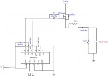

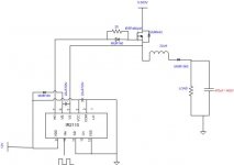
you must have a low impedance path for charging the bootstrap capacitor.
If your circuit is a buck converter, then you forgot to put a diode or a mosfet for preventing brutally inductor current interruption.
My suggestion is to add a low side mosfet. IR2110 is designed to work in a half bridge configuration.
If your circuit is a buck converter, then you forgot to put a diode or a mosfet for preventing brutally inductor current interruption.
My suggestion is to add a low side mosfet. IR2110 is designed to work in a half bridge configuration.
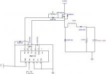
the diode in the mosfet's gate is connected in a wrong way. Usually mosfet turn-on (charging of gate-source capacitance) is done through a resistor (20Ohm in your case). Fot turning off, sometimes a faster discharge current is requred, so the gate resistor is bypassed by a diode.
Also, you can remove the diode after the inductor
Also, you can remove the diode after the inductor
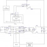
Actually my main application is as attached when there is a step up of load and the output voltage drops so the microcontroller detects the voltage drop and gives pulses to the mosfet and high voltage is injected to recover the voltage drop...
As from simulations i have succesfully got the result for this method ... but now the problems is switchiong the high side mosftet... any ideas or solutions are very much appreciated.
As from simulations i have succesfully got the result for this method ... but now the problems is switchiong the high side mosftet... any ideas or solutions are very much appreciated.
Attachments
you didn't understand how IR2110 works...
In a half bridge configuration, when the low side switch is in ON state, the bootstrap capacitor finds a low impedance path (through the mosfet) and charge to the driver supply voltage.
When low side switch turns OFF, the mid point between the two mosfets became floating, bootstrap capacitor being charged at vcc "above" floating point voltage.
Now, in your circuit, there's no way to charge the bootstrap capacitor because you do not have a low side switch (path). In this situation, you may consider an auxiliary circuit capable to generate the required floating voltages.
IR app note AN978 suggests a kind of a voltage doubler (figure 16)
http://www.irf.com/technical-info/appnotes/an-978.pdf
Everything is wrong. The IR2110 blows because there is no discharge path for the inuductor other than through the internal diodes of the own IC.
On the other hand, the isolated converter can regulate its output without additional switching regulators.
Furthermore, it seems that you are trying to switch non-isolated 300V from rectified mains to an isolated +/-25V output, which is completely crazy. Please give up ultil you learn enough electronics to know what you are actually doing
Actually the 300V that im trying to switch is isolated via a isolation transformer, sorry it was not stated clearly in the picture.
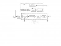
This method is to improve transient response . From the attached diagram, an additional parallel circuit denoted as VISI is connected to the conventional VMC control based SMPS. The parallel circuit consists of an isolation transformer, a bridge rectifier, a MOSFET switch, a filter inductor and a feedback control circuit. The isolation transformer with winding ratio of 1:1 is used to isolate the ac voltage to the output. The bridge rectifier rectifies the secondary voltage of the isolation transformer to obtain a high dc voltage. The dc voltage is switched in a similar manner as a buck converter. As usual the ripple of the output current is filtered using an inductor. The feedback control circuit receives output voltage as an input and produces gate pulse to the switch. This method is operated only during the transient operation of the SMPS.
Here in this method a high dc voltage from the input is injected to the lower inductance of the output filter inductor during step increase of load. Therefore, when a high dc voltage passes through a smaller effective inductance, the rate of change of current that is supplied to the load would be faster. during steady state condition the auxiliary converter does not come in.
Attachments
Dear All,
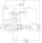
I have attached some changes, because as earlier the bootstrap capacitor is not charged..
At the beginning of the initial cycle during startup, the bottom-side MOSFET switch is turned on. This pulls the Vs pin to ground, which charges up the bootstrap capacitor to through bootstrap diode .
When the high-side driver is enabled during the next half cycle, the driver can turn on the high-side mosfet, and the Vs pin will rise up to VIN (0-300 V) .
Then the cycle repeats itself—high mosfet is switched off, bottom mosfet turned back on, the Vs pin is pulled down to ground, and bootstrap capacitor is recharged.
Attachments
The idea is pointless because the auxiliary control loop will not be able to react faster than the main control loop, particularly if it's controlled by a PIC with ADC latencies and calculation delays.
The own main control loop (frequency compensation and output filter) may be designed for optimum transient response without requiring additional loops.
The own main control loop (frequency compensation and output filter) may be designed for optimum transient response without requiring additional loops.
- Status
- This old topic is closed. If you want to reopen this topic, contact a moderator using the "Report Post" button.
- Home
- Amplifiers
- Power Supplies
- hide side mosfet driving