Hi, I finally succesfully built an off-line 250W Half bridge SMPS using as driver an IR2110, didn't blow up or anything taking the nessesary cautions...
Thing is, I correctly snubbed the FETs' switching noise with 2 RC snubbers (sorry, the only snubber I know for this topology), and the err amp compensation is ok (works fine in full range of voltage/current) but still in the DC side, the diodes (four MUR460) heat up pretty fast, even at low current, while the mosFETs (2SK2645) at 100W output, even with no heat sink, don't get even at 50ºC, I can touch them with no problem... Is the riging left that is making the diodes heat up so much? I've tried first with schottky rectifiers (MBR2045CTG) with big heat sinks, and looking at the transformer output I thought it might be because of the secondary voltage wich is 38V+ringing (approx 43.5V peak) so I changed them for the MUR460s, but the result is the same... I know the UF diodes are much slower than schottky rectifiers so... Will it make any difference placing MBR20100 instead? or I must reduce the ringing even more?
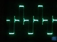
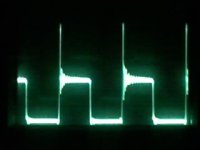
I attached the signal in 300V side and the rectified signal before the inductive filter
Thanx!
Thing is, I correctly snubbed the FETs' switching noise with 2 RC snubbers (sorry, the only snubber I know for this topology), and the err amp compensation is ok (works fine in full range of voltage/current) but still in the DC side, the diodes (four MUR460) heat up pretty fast, even at low current, while the mosFETs (2SK2645) at 100W output, even with no heat sink, don't get even at 50ºC, I can touch them with no problem... Is the riging left that is making the diodes heat up so much? I've tried first with schottky rectifiers (MBR2045CTG) with big heat sinks, and looking at the transformer output I thought it might be because of the secondary voltage wich is 38V+ringing (approx 43.5V peak) so I changed them for the MUR460s, but the result is the same... I know the UF diodes are much slower than schottky rectifiers so... Will it make any difference placing MBR20100 instead? or I must reduce the ringing even more?
I attached the signal in 300V side and the rectified signal before the inductive filter
Thanx!
Attachments
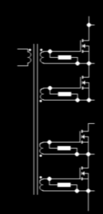
maybe the high side mosfet is not properlly driven.
it is a big problem to drive this floating GS junstion, and that's why i use a hand made transformer to drive the two mosfets.
how to do this driver?
very simple and easy:
take a toroid, build one primary with 10 turns, and as many secondaries as you have mosfets to drive with the ratio 1:1
put a 10k resistor before GS junction.
put clamping diodes on primary winding.
then, it will be a very simple cheap transformer.
Attachments
Hi chimi
After getting the schematic, we'll sort out properly. But I think, your transformer winding may not be very good and thus leakage inductance is producing spikes, which is heating the diodes. You could rewind your transformer for minimal leakage inductance and maybe, add an RC snubber after the transformer before the diodes.
Thanks.
Hi everyone and thank you very much for your answers...
To start with something, yes, the transformer may be not specially good, since it is a hand-wound toroid, I did my best, with multifiliar wounds and everything, but it still may not be enough...
Regarding the driver (IR2110) I have some particular experience with them, besides I've been properly advised by the people at International Rectifier, and I have some advanced app notes from IR to use them, so, I don't think the driver is the problem here, what I can appreciate, is that the assimetry is produced when the low side is induced... if you look at the primary waveform, you can see this clearly, the amplitude of the high side is 152V approx and the low side amplitude is 135V approx, can it be the capacitive divider??
About the snubbers, I only have across the primary side mosFETs, and are very primitive RC snubbers, but they seem to accomplish more or less what they have to, maybe smaller resistor will suppress a little more ringing... what I didn't unerstand is the snubbers for the secondary (or output) side diodes, didn't know about them, how are the placed in the circuit?
About the schematic, let me first get it a little smoother for you to understand it, it's a real mess... I'll post it later
Thanx!!!
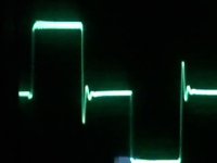
I corrected the imbalance in the waveform by removing of the circuit a resistor and a capacitor which are preventive for voltage undershoot when using IGBTs since this SMPS does not use any IGBT
Also I reduced the 1K2 resistor of the snubber to 820 and the ringing freq damped from 6Mhz to 2Mhz
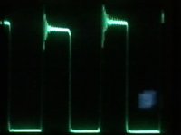
Here I attach the pics of the primary waveform (27-10-08_1239.jpg) and the transformer output waveform rectified before the inductor filter , in this one, you can see the effect of leakage inductance in the secondary side, this surely needs that snubber, please tell how to place it!!!
Thanx
Also I reduced the 1K2 resistor of the snubber to 820 and the ringing freq damped from 6Mhz to 2Mhz
Here I attach the pics of the primary waveform (27-10-08_1239.jpg) and the transformer output waveform rectified before the inductor filter , in this one, you can see the effect of leakage inductance in the secondary side, this surely needs that snubber, please tell how to place it!!!
Thanx
Attachments
i would try to improve the coupling first before trying snubber the ringing , if you place one secondary on top of the other one then try to place both of them side by side, its like you take 2 wire and wind both secondary at the same time, a diode can be snubbed by placing a snubber across it
I wound the transformer on an EE core, first winding: half primary; on top of it the whole secondary with central tap (2 equal secondaries of 3 wire each) and finally the other half of the primary.
The results were somewhat better than before but the diodes still heat up
Can someone please post the schematic of how I put the snubber across the output diodes??
Thanx
Regard, Fernando
The results were somewhat better than before but the diodes still heat up
Can someone please post the schematic of how I put the snubber across the output diodes??
Thanx
Regard, Fernando
Well, the switching frequency is 125 KHz, Bmax=0.2T, in the PCB design, everything is single point grounded, and the primary side is optically isolated from the output, grounds are not coupled yet.
The transformer is winded like this
o : primary wire
x : secondary wire
oo oo oo oo oo oo oo oo oo oo oo oo oo oo oo oo oo oo oo
oo oo oo oo oo oo oo oo oo oo oo oo oo oo oo oo oo oo oo
oo oo oo oo oo oo oo oo oo oo oo oo oo oo oo oo oo oo oo
oo oo oo oo oo oo oo oo oo oo oo oo oo oo oo oo oo oo oo
-------------------------------------------------------------------------
xxxxxx xxxxxx xxxxxx xxxxxx xxxxxx xxxxxx xxxxxx xxxxxx
xxxxxx xxxxxx xxxxxx xxxxxx xxxxxxx xxxxxx xxxxxx xxxxxx
-------------------------------------------------------------------------
oo oo oo oo oo oo oo oo oo oo oo oo oo oo oo oo oo oo oo
oo oo oo oo oo oo oo oo oo oo oo oo oo oo oo oo oo oo oo
oo oo oo oo oo oo oo oo oo oo oo oo oo oo oo oo oo oo oo
oo oo oo oo oo oo oo oo oo oo oo oo oo oo oo oo oo oo oo
A while later I'll post the schematic
Thanx
- Status
- This old topic is closed. If you want to reopen this topic, contact a moderator using the "Report Post" button.
- Home
- Amplifiers
- Power Supplies
- Half-bridge heat problems