Hi everyone... I'm starting a new push-pull smps design and I don't want to use the old TL494 again, want something that allows current mode control and honestly I don't know or used for this topology any other PWM. I used to put a BJT totem pole to drive the MOSfets, but would be cool not to... by the way, the TL494 has 2 error amps, can one of the be used as a current ramp limit anyway, is it wise??
Getting back to the main issue...
1)which PWM IC should I use/would be best for a 2 voltage output push-pull from 230Vac to 24Vdc 4A and 12Vdc 1A...
2)Being the total output power approx 110W... Is it wise to make this out of a flyback considering that here in Argentina, the only gapped option I have is an EE2507 core with a 0.5mm gap?
3)I designed in the past a 70W flyback using this core at a switching freq of 100KHz, would be a lot more difficult to redesign with this core at 200KHz sw freq? would the compensation network be a lot more complicated?
Thanx!!!
3 viable choices
A 2-switch flyback would be a good approach as well as a 2-switch forward. Also worth considering is a half bridge. At 230V ac input, a push-pull center tap, or PPCT, is not a good choice. The PPCT places a voltage stress on each FET equal to twice the supply rail. With 230V ac, the max is 264V ac, which when rectified can reach 373 volts. Doubling gives 746 volts, requiring the use of 1000V FETs. Selection is limited. Also, clearance requirements would be needed for 746 volts. The same applies for a 1-switch flyback or forward.
With a half bridge, HB, 2-switch forward, 2SFWD, or 2-switch flyback, 2SFBK, the stress on each FET is one times the supply rail, or 346V. Thus 500V FETs easily do the job, and the clearance requirements are half of the PPCT case.
At high line inputs such as 230V ac, the last thing we want to do is double the voltage. At a power level of 110 watts, the HB is overkill, but still a viable choice. The 2SFBK is very suitable, but flybacks are noisier than forwards, and tend to place high peak stresses on the components. The 2SFWD is a very good method. It is quiet, fast, and places moderate stress on the parts. I hope this helps.
Please be very careful with 230V ac!
Helps a lot...
I have a reasonable doubt, I've built simple dual- swicth push-pull converters and the voltage stress over the mosfets was just the rail voltage, the exact double is with a single switch forward converter, that on one side has the rail voltage and when switches off on the other side has rail voltage inverted discharging the flux induced by the first primary during on time, thus, stressing with doubled voltage...
I have reasons not to use half-bridge in 300V+, it is very difficult to configure bootstrap components for the driver (I.E. IR2110) and eventually blows up pretty badly...
I never seen or used a dual switch flyback, but I succesfully produced a 70W flyback fresh from 230Vac to 19V 3.5A with only one switch, look at my next post "110W flyback" where is an schematic of that 70W flyback, was somewhat noisy but was very cheap....
There is nothing wrong with the PP current mode topology....
Yes it does have twice the stress + transients...but that kind of thinking was from the 70's and or from reading all the outdated SMPS books that are still popular..... The FETS today are available in high voltage for reasonable prices and descent Rds-ON....
Thats unless your building for production and your a typical "cheap" engineer who won't spend a penny more than you have to.....
I would recommend useing LT chips and avoide the old UNITRODE dies chips from the 80's....such as the 1845's and thier derivatives, since th error amps in these controllers are pittyfull...
Chris
cerrem said:There is nothing wrong with the PP current mode topology....
Yes it does have twice the stress + transients...but that kind of thinking was from the 70's and or from reading all the outdated SMPS books that are still popular..... The FETS today are available in high voltage for reasonable prices and descent Rds-ON....
Thats unless your building for production and your a typical "cheap" engineer who won't spend a penny more than you have to.....
I would recommend useing LT chips and avoide the old UNITRODE dies chips from the 80's....such as the 1845's and thier derivatives, since th error amps in these controllers are pittyfull...
Chris
Sorry to differ, but yes, there is something wrong with PPCT at **high voltages**. The info I give is current, not '70's or '80's.
The fact that 900 and 1000 volt MOSFETs are available is not a reason to use a PPCT. I know that such devices are available. With 230V ac input, the PPCT doubles the voltage and as a result, the creepage requirement and clearances on the pcb is that of nearly 800 volts. Larger spacings means less available board space. Larger creepage means less of the transformer window available for winding.
The PPCT finds its home in low voltage applications, 12, 24, 48V etc. It is not a 230V solution. The loss due to Qoss increases as the square of the voltage, as well as snubber loss. The turn on and turn off loss increases w/ larger voltage. The Rdson of a 1000 volt device is at least twice that of a 500 volt part. The HB and the 2-switch flbk and frwd topologies are more suited to higher voltages. So is the full bridge, but FB is overkill for just 110 watts.
The most appealing feature offered by the PPCT is that both MOSFETs are low side driven. N-channel parts can be used with no high side drive headaches, i.e. no bootstrap, charge pump, or level shifting required. All of the others mentioned require driving at least one high side MOSFET. At high inputs, i.e. 230V ac, this can be tricky. Negative gate drive may be needed as well as capacitive Miller clamping to prevent false turn on due to dv/dt. For high voltage offline ac applications, the PPCT is seldom used. It does offer simplicity regarding FET drive, but the other problems outweigh this benefit.
Again, a PPCT could be made functional. If FET gate drive is too difficult with the other topologies, the PPCT does make that problem disappear. BR.
Guys, your helping me a lot from your discussion because
1) Yes, I dont want to have high voltage stress over the FETs, and I prefer if nesessary to use a high side driver than stressing high voltage mosfets with the restpective very high voltage transient, not to mention difficult to snub.
2) Well, I'm a relatively cheap engeneer, not for my own reasons, in this country, the cost of a power supply must tend to zero, but I'm not that cheap, not cheap enogh to jeopardize people and so on, the only reason I rather not to use very high voltage mosfets is their relatively high Rds on, wich increases the heak-sink price, wich in this country, is real big, its better to add extra silicon than heat sinks.
3) I've made REAL-basic schematics of what I understand were the topologies discussed in this post, except for dual switch forward, in that you got me, don't know anything about it, and I'd like to know what are the benefits of using a dual switch flyback or dual-switch forward (from now on 2sfb and 2sfw as you called them), my guess is the option to decide between ZVS and ZCS...
Attachments
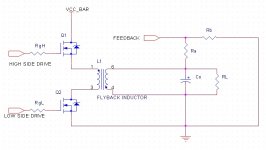
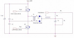
I know in the flyback is missing the output diode, my mistake, did this pretty fast, sorry, but the idea shows.
Hope you can get me a schematic of a 2SFW converter and tell me about its upsides and drawbacks I.E. Is the voltage stress the double than the line voltage) and so on. And...
Which ICs replace the old 1845 and it's derivates, I know for certain that the err amp is terrorific in those...
Thanx to you both
Fernando
Chris: Making and analisis of the gain and transient response of the prior boost converter I've (don't know if you remember) I made the load regulation pretty solid, thanx
chimi said:Helps a lot...
I have reasons not to use half-bridge in 300V+, it is very difficult to configure bootstrap components for the driver (I.E. IR2110) and eventually blows up pretty badly...
There is nothing inherently wrong with IR2110 and IR2113. If the circuit blows you are the one doing something wrong.
sorry eva, that's what usually happens, I do something wrong!!!! can you help me design a bootstrap config for the 2110 (the only one aroung here) if you got some experience using it, because the only one I got steady working with no blowups was at 120Vca and before it was working I blew one too because it latched internally (my guess after seeing what was left of the circuitry) due to small bootstrap caps...
Please show us your PCB layout. Realiability has a lot to do with it.
To filter gate transients (that could cause latching or damage) I use ferrite beads of various sizes rather than resistors (that also control turn on and turn off times). To prevent negative bias of the high side driver I use low inductance layout and RC snubbers (to prevent strong ringing or just "single cycle" negative overshoot).
To filter gate transients (that could cause latching or damage) I use ferrite beads of various sizes rather than resistors (that also control turn on and turn off times). To prevent negative bias of the high side driver I use low inductance layout and RC snubbers (to prevent strong ringing or just "single cycle" negative overshoot).
Eva said:
There is nothing inherently wrong with IR2110 and IR2113. If the circuit blows you are the one doing something wrong.
Yes, the probelm with those chips is they can't tolerate any sort of fault in the circuit they're driving. I have an application (pulsed test of high power RF amplifier ICs) where NO form of current limiting can be used because too much impedance between the reservior caps and the DUT causes the DUT to go unstable. We blow the stupid driver chip out all the time when a DUT goes south. Current limit on the mains supply prevents fires and most of the time the hexfet survives. But we keep spare drivers close at hand. The problem with SMPS development is that conditions like that can exist in the concept/design phases and chips will be blown.
A 0.5A fast blow fuse in series with the gate is something that I'm considering for future designs. It may be effective when the gate becomes shorted to the source, or even when the source bonding wire opens and the gate becomes shorted to the drain. In the first case, limiting the supply current to the driver IC also works fine.
"I have an application (pulsed test of high power RF amplifier ICs) where NO form of current limiting can be used because too much impedance between the reservior caps and the DUT causes the DUT to go unstable."
What about a small Ferrite bead in series with the Gate output?
The other choice is to use beefer gate drivers. IXYS makes high current gate drivers:
http://www.ixyspower.com/store/Family.aspx?i=63
IX6R11P7 6A MOSFET (IR2113 compatible)
http://ixdev.ixys.com/DataSheet/DS99037.pdf
What about a small Ferrite bead in series with the Gate output?
The other choice is to use beefer gate drivers. IXYS makes high current gate drivers:
http://www.ixyspower.com/store/Family.aspx?i=63
IX6R11P7 6A MOSFET (IR2113 compatible)
http://ixdev.ixys.com/DataSheet/DS99037.pdf
Eva: I haven't started the design yet, so I have no PCB layout, however, after so many bloups, I spoke with a representative of IR which gave some guidelines and so I managed to build a 110Vac app: A 230W HB that did never blow, but the voltage is pretty different (165Vdc against 310Vdc) from that we're speaking about, and after at least 8 bloups in 230Vac let's say "me acobardé" and then I tried aboiding this topology until these days
Lets do something, for tomorrow or the day after I'll post a schematic of a HB design, following basic rules that are in a pdf I'll post now and other app notes in PDF that can't post due to their size called AN-978 and DT04-4 revA about IR2110 and the we'll see
Regards and thanks to you both for Ur concern
See you
Attachments
I'm using IR2113 to switch 420V at turn on, 580V at turn off and 32A peak and I can say that it's reliable. I had to use RC snubbers from drain to source to slow down turn-off crossover times a bit because they were exceeding the 50V/ns limit, and to damp a mild parasitic resonance at >50Mhz that was resulting in increased amplitude on negative gate spikes (more than -10V before the ferrite bead, -1V after the bead). These spikes are produced by source lead inductance.
You must check all waveforms with an oscilloscope capable of showing 100Mhz with little attenuation (ok, I don't check high side gate waveforms because this is a very difficult floating measurement). Triggering the oscilloscope with the input signal to the IR2113 makes things easier because the delay of the IC is usually longer than the trigger delay of the oscilloscope thus allowing to see the complete turn-on and turn-off events.
Waveforms should be checked in all operating modes (idle resonant mode, positive output current with reverse recovery on low side body diode and negative output current with reverse recovey on high side body diode). Undamped ringing is an easy way to put stress on the gate driver IC because the voltage across source lead inductance is fed to the gate driver output (and this inductance is almost always part of the RLC tank that produces ringing).
- Status
- This old topic is closed. If you want to reopen this topic, contact a moderator using the "Report Post" button.
- Home
- Amplifiers
- Power Supplies
- push-pull PWM IC