Hi,
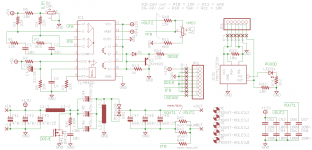
I designed the following SEPIC converter for experiments with the solar panels I'm soon buying. The schematic diagram, both copper drawings and the assembly drawing are added to this message. The solar panel system I spoke of consists of two 100 W panels (Voc~20 V, Isc~10 A), so one knows pretty sure the worst case conditions. Basically, you cannot draw more current from the panels than the rated short circuit current is.
Anyway, this converter works perfectly when there is a small load at the output (the output voltage is set to 14.4 V). But when I start to draw more current through the converter from a 12 V test supply, an irritating noise appears, and it gets louder as the current increases. So I thought the inductor core must be saturating. It isn't maybe made clear in the schematic, but the two inductors are wound on the same core, E42/21/20 with approx. 3 mm air gap (quite large one). I tried to simulate and calculate the inductors and core to withstand maximum of 10 A, but something has gone wrong. The inductors consist of 15 turns, two 1.2mm (diam.) enamelled copper wires wound parallel.
I fear I have made one crucial mistake: I salvaged this core from a defective SMPS, and it might be that the ferrite core itself is permanently magnetized and therefore saturates far more easily. I could fix it if I heated the core above its Curie temperature, but since that isn't an option, I guess it's time to make a new inductor set. Could there be any other reason for premature saturation? Thanks for opinions!
The schematic
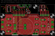
The bottom copper
The top copper
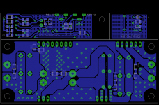
The assembly
I designed the following SEPIC converter for experiments with the solar panels I'm soon buying. The schematic diagram, both copper drawings and the assembly drawing are added to this message. The solar panel system I spoke of consists of two 100 W panels (Voc~20 V, Isc~10 A), so one knows pretty sure the worst case conditions. Basically, you cannot draw more current from the panels than the rated short circuit current is.
Anyway, this converter works perfectly when there is a small load at the output (the output voltage is set to 14.4 V). But when I start to draw more current through the converter from a 12 V test supply, an irritating noise appears, and it gets louder as the current increases. So I thought the inductor core must be saturating. It isn't maybe made clear in the schematic, but the two inductors are wound on the same core, E42/21/20 with approx. 3 mm air gap (quite large one). I tried to simulate and calculate the inductors and core to withstand maximum of 10 A, but something has gone wrong. The inductors consist of 15 turns, two 1.2mm (diam.) enamelled copper wires wound parallel.
I fear I have made one crucial mistake: I salvaged this core from a defective SMPS, and it might be that the ferrite core itself is permanently magnetized and therefore saturates far more easily. I could fix it if I heated the core above its Curie temperature, but since that isn't an option, I guess it's time to make a new inductor set. Could there be any other reason for premature saturation? Thanks for opinions!
The schematic
The bottom copper
The top copper
The assembly
Well, I did make several changes today:
-Added RC snubbers across the diodes
-Added 1 uF in parallel with the compensation loop capacitor
-Added 100 nF between Vfb and ground
-Added 1 uF between Out and ground directly after the diodes
As a result the waveforms and behaviour improved a bit. The voltage over the diodes shows still some oscillation, although rapidly damping. I can take only approx 0.5 A from a 12-V supply until the input current begins to increase and the horrible noise appears.
Could someone give any hint on this issue? Is the layout ok?
The "horrible noise" is the result of quick duty cycle changes due to control loop oscillation. This happens when frequency compensation is wrong. I don't have any experience with SEPIC and I don't know how you derived your compensation scheme, but there may be some mistake.
Also, two 1000uF 16V capacitors in parallel don't seem enough at all to reliably handle the ripple currents involved for 15A output, even if they are of the low-ESR type.
Also, two 1000uF 16V capacitors in parallel don't seem enough at all to reliably handle the ripple currents involved for 15A output, even if they are of the low-ESR type.
Though SEPIC is a bit uncommon to use as solar array preregulator, I'm interested if you could post your findings if you make the thing work.
Bear in mind that a solar array essentially works as a voltage limited current source, and the most accurate model is to use a current source with diodes antiparallel and a series resistance.
Texas Instruments (formerly Unitrode) prepared some good reference design papers on SEPIC. Try a search on reference "SEM900". There are some links left to the control loop design.
Good luck!
Bakmeel
As both sections of L1 are wound on the same core (as is possible to do with SEPIC), the ripple current through the 2x1000uF caps is much reduced compared with the case where the inductors are seperate. The values shown should easily be ok. (In my limited experience with SEPIC that is!)
SEPIC is complex
It sounds like control loop instability. A SEPIC is a complex topology, and not trivial when it comes to compensation. At light load it operates in discontinuous mode, and should be stable. But, if it enters continuous mode, at heavier load current, stability becomes complicated.
Dr. Ridley on his site "Switching Power Magazine" has a good paper that covers the SEPIC issues. I'd recommend downloading, as it is free. The SEPIC in continuous mode has a small signal transfer function with 2 pairs of complex conjugate poles (4 poles in all), as well as 3 right half plane zeroes. The only way to compensate and achieve stability with 7 lagging singularities would be to limit the loop bandwidth to a frequency less than the upper complex pole pair, or lowest right half plane zero, whichever is *lower*. The end result is usually a converter with very limited speed. Transient response due to sudden changes in load or input will be impaired. With 4 poles and 3 right half plane zeroes, the total phase lag approaches 630 degrees!
I've designed close to 100 SMPS, and my converters are in millions of products worldwide. I have never used the SEPIC topology for reasons above. A good careful design using the SEPIC topology can be done. One simply must be careful. For up/down conversion sans isolation, I use the non-inverting buck-boost (NIBB) topolgy. It has 2 FETs and 2 diodes vs. 1 FET and 1 diode for the SEPIC. The efficiency of the NIBB is slightly less than that of the SEPIC, but the speed is much better. The NIBB in continuous mode has only 1 pair of complex conjugate poles, and 1 right half plane zero. Stability is assured by limiting the control loop BW to less than the right half plane zero frequency.
I hope this helps.
Hi all,
thanks for your opinions, I really appreciate them! Currently my spare time is limited, so it will take a while before I'm able to look into this matter.
It should be evident by now that I'm merely a beginner with the practical part of switching power supplies, but I did not implement current-mode control for several reasons: First, it was easier this way. Second, I was under the impression that current-mode control was useful mostly because of the current limit capability and faster transient response. I was'nt aware of it's effects on the control loop stability.
I haven't posted any pictures of the converter, but the control IC and most of the resistors and caps related to it are placed on a small separate board which is attached vertically to the main board. Very much in a way that many off-line converters are build. I did it just for the reason that it would be more easy to change the control circuitry if needed. Now the urgent need has risen, so I only need to define a stable control loop, not to design a whole new board.
Some progress made:
The following files show the Pspice & SwitcherCAD models I used to tackle this compensation obstacle. What I have recently done is:
-I made spice model from the UC3842 error amplifier
-Plotted the magnitude and phase responses of the initial circuit (the one with the stability problems)
-Added RC filter to freeze the magnitude response much earlier in the frequency range
-Plotted the responses once again, noting the possible improved performance
-Used the LTSpice model to see if any improvement happened
It seems that this converter should now work a bit better. I read the article Mr. Claude Abraham kindly told about and that prompted me to try the radical decrease in magnitude response. For now, it worked. Haven't tried fixing the physical circuit yet.
Here are the files:
-The pspice model of the initial feedback loop
-The pspice model of the corrected feedback loop
-The initial frequency response plot
-The corrected frequency response plot
-The initial gate voltage waveform
-The corrected gate voltage waveform
-The LTspice model of the converter
p.s. Don't pay too much attention to the error amp model, it may not be accurate enough when it comes to input/output impedances, I tried to make the frequency responses equal with the ones on the datasheet.
If you look at the initial gate voltage waveform, I can tell you that it indeed look exactly like that when observed with a digital scope! I really hope to get this converter operating soon!
Here are results from a 5A pulse-loading simulation:
5A pulse load response
The converter is loaded with two 5 A pulses, duration 30 ms each. Load rise/fall times are 10 ns. These load pulses are visible on the pdf, but they are not well visible.
The output voltage follows the suden load chage nicely, perhaps more than I expected. The settling time should be enough for my purposes. But still, the converter doesn't like a similar 10 A load. I would blame the controller, since the controller ouput duty cycle reaches approx. 70 % maximum instead of the near 100 % promised in the datasheet.
Could there be something in the compensation loop that reduces the maximum duty cycle?
Hello!
Good news at last: I fixed the compensation network as previously described and now the converter works quite well") . As Dr. Ridley stated (or someone else, cannot remember), this converter is very slow. This can be verified with a large, sudden change in load. Practically my converter isn't able to handle sudden loads below ~15 ohms (Vout=14.4 V, Vin=12 V). But if I gradually increase loading, I can go down to 10 ohms - but not further.
. As Dr. Ridley stated (or someone else, cannot remember), this converter is very slow. This can be verified with a large, sudden change in load. Practically my converter isn't able to handle sudden loads below ~15 ohms (Vout=14.4 V, Vin=12 V). But if I gradually increase loading, I can go down to 10 ohms - but not further.
I'll post here again once I've conducted more precise measurements with that lovely 4-channel digital scope at work Thank you all for help and support!
Good news at last: I fixed the compensation network as previously described and now the converter works quite well
. As Dr. Ridley stated (or someone else, cannot remember), this converter is very slow. This can be verified with a large, sudden change in load. Practically my converter isn't able to handle sudden loads below ~15 ohms (Vout=14.4 V, Vin=12 V). But if I gradually increase loading, I can go down to 10 ohms - but not further. I'll post here again once I've conducted more precise measurements with that lovely 4-channel digital scope at work
Thank you all for help and support!upping a 4 year old thread. Here's my story
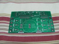
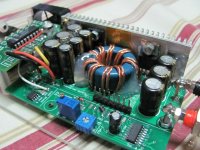
I'm building a SEPIC based CC/CV mode switchmode supply for various applications so I designed and had boards made. some of my planned applications are battery chargers and LED drivers. (see attachments for PCB layout and schematic)
The board uses the ancient TL494 (as I already had a bunch of those) for PWM control, IRFZ44 as the main switch. Hi-Flux core for the main inductor, all Panasonic FM for the input, output and sepic caps, MAX4172 for the high side current sense (can eliminate that and use a low side current sense resistor if output ground doesn't have to be the same as input ground)
The problem:
First application I have for it is a 15Ah LiFePO4 battery pack charger which needs about CC at 3A and CV at 14.60V.
I'm having a really hard time stabilizing the circuit. The CV mode is fine, transient response works well with a small overshoot and there's a small lag at no load to full load response.
in CC mode, current is maintained but the circuit goes crazy and makes buzzing noises. I've been working on and off on this thing for about two weeks until I stumbled upon this thread and the mentioned app notes. Ended up having to add a snubber (3K + 1uF) across R32 to slow down the response greatly.
Once it was slowed down, circuit behaved perfectly. It's actually fine since the load does not need a fast response since in battery charging, the voltage and current does not change quickly. One minor problem I have is that if the circuit is powered before the battery is connected, once battery makes contact, there is a huge current spike as it takes a bit before the current limiting takes effect. If the battery is connected before power applied to the circuit, there is no problem as the circuit has soft start implemented on the TL494.
I can post pictures of the actual unit if someone's interested.
Attachments
I forgot to add:
The point when the circuit goes crazy is at moderate loads. It occurs well below the point where the circuit goes from discontinuous mode to continuous mode but I tried another coil with more turns and still occurs at approx same current level.
At first, when I wound the inductor using single #18 wire per winding then switching to 20 strands of #31 wire per winding made things much better but the oscillation in current mode persisted but much much less than the single #18 wire. Turn counts were the same. Switching frequency is around 56kHz. I couldn't explain how that happened. It must have something to do with better current flow due to the litz wire at high freq and high current but I don't know much more.
Then I also noticed that the instability occurs at about >2.7A input current. if I increase input voltage or decrease output current limit threshold to maintain 2.7A input current, the circuit is stable without the RC snubber across R32.
The PCB also has options to be used as a boost converter but I don't have immediate application for that so it is not yet tested for that use.
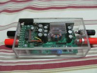
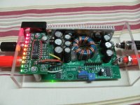
The converter works pretty well now so I made an acrylic box for it.
output is set at 14.4V and current limits at 3A
I can use it for charging the 15Ah LiFePO4 battery pack or providing a constant 14.4V supply for loads under 3A with a 10V-18V input.
*reposted because I uploaded the wrong size pictures*
output is set at 14.4V and current limits at 3A
I can use it for charging the 15Ah LiFePO4 battery pack or providing a constant 14.4V supply for loads under 3A with a 10V-18V input.
*reposted because I uploaded the wrong size pictures*
Attachments
- Home
- Amplifiers
- Power Supplies
- Difficulties with SEPIC converter