Hi everyone I am new at this forum!!!
I am designing a boost regulator to get 15Vdc-4.4A from the +12Vdc from the PC PSU. Thing is that I seem to fail somewhere in the design of the error amp compensation network, first of all I want you to know that everything is free of noise and well snubbed with RCD snubbers so the are apparently no current transcients when switching on
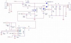
The circuit uses a current mode IC: the famous UC3845 and the MOSFET is an IRFZ44N which has a RDSon=17.85 mOHM which is close to ideal
the configuration of the compensation network is the typical 1 diode and 1 resistor paralleled that some authors call "single pole with in-band gain", no optical isolation (obviously).
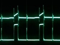
What happens: some of the switching pulses (normally 1 out of 2) are stopped just at turn on time, thus having almost no switching for the entire cycle, at first glance I thougth It was the current sense, but the transient in the on periods that happen with no problem are really bigger than those truncated, so, I don't think so....
I attached a picture of this seen on my oscilloscope so you can get the whole picture
Thanks!!!
I am designing a boost regulator to get 15Vdc-4.4A from the +12Vdc from the PC PSU. Thing is that I seem to fail somewhere in the design of the error amp compensation network, first of all I want you to know that everything is free of noise and well snubbed with RCD snubbers so the are apparently no current transcients when switching on
The circuit uses a current mode IC: the famous UC3845 and the MOSFET is an IRFZ44N which has a RDSon=17.85 mOHM which is close to ideal
the configuration of the compensation network is the typical 1 diode and 1 resistor paralleled that some authors call "single pole with in-band gain", no optical isolation (obviously).
What happens: some of the switching pulses (normally 1 out of 2) are stopped just at turn on time, thus having almost no switching for the entire cycle, at first glance I thougth It was the current sense, but the transient in the on periods that happen with no problem are really bigger than those truncated, so, I don't think so....
I attached a picture of this seen on my oscilloscope so you can get the whole picture
Thanks!!!
Attachments
But it is a boost converter, and before actually mounting the snubber in the PCB, at a 3A load, the noise was enough to make the inductor sound due to fast-changing duty cycle, the inductor current sense was crazy
After I single-point grounded the control logic and all of its external components, the supply works fine in light loads (0.5 to 2A) but at 3A and above I experience this problems again, not as severe as before, but it doesn't do any good anyway
Thanx!
After I single-point grounded the control logic and all of its external components, the supply works fine in light loads (0.5 to 2A) but at 3A and above I experience this problems again, not as severe as before, but it doesn't do any good anyway
Thanx!
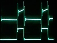
As crazy as it sounds (at the beggining) I tried removing the snubbers and the supply worked just fine, I posted a pic of the stable switching after the removal of the snubbers.
I reached the conclusion that there was no need of a snubber and the single point ground for the logic was crucial, so before I implemented the single point ground, the snubber was "needed" because all the noise ended up in the logic, but afterwards only increased the voltage transcients over the sense resistor
You were right, thanks, you do not know how much I needed this to work
Attachments
You still need to examine the closed loop response of the system..
You can measure it on the bench...
But first it is advisable to get out the BODE plot semi-LOG paper.
Derive and draw out the OPEN-LOOP response, then your ERROR-AMP response....then you can see your CLOSED-LOOP response... Check your PHASE MARGIN and GAIN MARGIN....if they are not within spec, then re-adjust ERROR-AMP values....
Also...watch out for the variation of LOAD, which may put you in DISCONTINOUS or CONTINOUS MODE transisitions, this can introduce a RHPZ (Right Hand Plane Zero) which may put the loop unstable....
Chris
Well...
I already tested abroad with a very fast-changing load: a 600Hz PWM switching over a 5A load all the range from 10% duty cycle to 100%, and works just fine, never goes in continuous mode.
Regarding closed loop response there are a lot of this I've got to learn, how to make a bode plot of phase and gain margin, this always was difficult for me, in high-school and in college... so I only do what I can with bibliography about power supplies on how to calculate just the components of the compensation network.
Regarding input filtering, i decided to try first without, see what happens and then mount the caps or not, and, seeing this works just fine, didn't put it in the circuit though, what I did not include in the schematic was a filter at the track just in the supply Vcc of the 3845, which is a series 12 Ohm resistor from the +12V followed by a 100uF aluminum electrolythic cap, which made really better the waveform of the out pin and the gate signal.
And finally the snubbers: I designed before no other thing than off-line supplies. generally flyback and push-pull and only one half-bridge, always isolated by the well known TL431 and the 4N25/35 opto, in this designs, a snubber was always needed because of the high RDSon and output capacitance of the 500V/600V transistors, in fact I tried all kinds of normal and lossless snubbers to see which was better for each of these topologies, even implemented a lossless snubber for the push-pull similar to that used in a flyback or a single switch forward converter, so, when I had instability in this particular circuit I thought "well, let's mount the snubbers" didn't know this would be a problem....
Thanks to you all !!
I'm still worried about closed loop response, I'll get deep into that
Regards!
Snubbers are important to help damp the ringing....
Choosing the optimum size for snubber is critical....and make sure to include the tolerance of the components for End-Of-Life and temperature as well....
If the snubbers are too big, they will have such a huge time constant, it will interfer with the switching time as you have already experienced...
The "quick and dirty" way to look at loop stability is to do a 10% to 100% step in the load and check the response with scope display for ringing and settleing time... Adjust as needed...
Chris
Thanks Chris for all the help
The snubbers I used before in the circuit were calculated using some design criteria from a book called "Power supply cookbook" from Brown, which doesn't honor its name because its no cookbook, its a great book, but the snubbers section is quite incomplete so... well I did what I could...
If some of you are interested I'll update the PCB with all the changes and then post it
Regards!
chimi said:Thanks Chris for all the help
The snubbers I used before in the circuit were calculated using some design criteria from a book called "Power supply cookbook" from Brown, which doesn't honor its name because its no cookbook, its a great book, but the snubbers section is quite incomplete so... well I did what I could...
If some of you are interested I'll update the PCB with all the changes and then post it
Regards!
No offense to Mr. Brown, but that book is not on my list to recomend... It is bad for a begginer since it leaves out way too much info and can get a begginer in trouble real fast.... It is too simplistic and incomplete for advanced designers...There are mistakes in some of the equations...So I have no idea what to use that book for???
To properly derive snubbers... the equations are lengthy and you must include all parasistics including trace analysis... also proper modeling of the FET's, claculating winding leakage inductance and winding capacitances .... Since I do this alot at work, it goes by quick since i have models set-up ready to modify and run...
The quickest and best approach in your situation is simply to "MONKEY" with the snubber value while looking at the waveform on the scope in the lab.... You want to tune the snubber to just smooth the glitch out, but not too much to kill the fundamental waveform shape or amplitude....remember to note the tolerance of the component and add that to the component value for your final selection.....
Chris
So, what book should you recommend for begginers that have succesfully built several supllies but want to learn a lot about compensation and noise snubbing, filtering, etc (such as me), taking for granted that for now I know enough about the inductors and transformers I need to build, but don't know how to calculate parasitic inductance...
Another question: what is to "monkey" with the snubber values and, seems to me that for a turn-off snubber is better a RCD , but for a turn-on snubber in this case RC is OK, is this a right tought?
Thanks for all, Fernando
Another question: what is to "monkey" with the snubber values and, seems to me that for a turn-off snubber is better a RCD , but for a turn-on snubber in this case RC is OK, is this a right tought?
Thanks for all, Fernando
chimi said:So, what book should you recommend for begginers that have succesfully built several supllies but want to learn a lot about compensation and noise snubbing, filtering, etc (such as me), taking for granted that for now I know enough about the inductors and transformers I need to build, but don't know how to calculate parasitic inductance...
Another question: what is to "monkey" with the snubber values and, seems to me that for a turn-off snubber is better a RCD , but for a turn-on snubber in this case RC is OK, is this a right tought?
Thanks for all, Fernando
Ok...
To "monkey" means that you adjust something by examination on the the bench, as opposed to doing it analyticaly by derivation of equations...
As for good power supply books.... I don't know of any that are up to date with the times anymore...they are old and outdated along with the old UNITRODE notes.... Such would be the book by Pressman...
The best way to learn SMPS is to learn from the best, the forefathers of SMPS... Search the internet for papers by Middlebrook, Vatche Vorperian,Cuuk, Dr. Ridley, to name a few.... These are the Caltech gurus...as well as Viginia Tech.... I had the pleasure of meeting them....
Learn the State-Space-Averaging techniques.....this is important..
Chris
- Status
- This old topic is closed. If you want to reopen this topic, contact a moderator using the "Report Post" button.
- Home
- Amplifiers
- Power Supplies
- problems with compensation in boost regulator