Hi.
I've been tweaking this design for quite a while now, and want to run it by the DIY community for feedback or suggestions. I have not built it yet, for lack of parts.
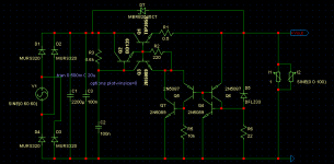
This isn't really intended for anything serious, I just started designing to see how well I could do. I figured that in the end I would have a nice lab supply with minimal ripple. Output is around 33VDC but can be changed by using a different zener diode. Adjustable Zener circuits work but not as well as using a single zener.
Rather than a capacitance multiplier, I decided I would go more the route of a specialized (super-sensitive) error amplifier keeping the output voltage steady.
If you want higher current you will need to lower the value of R3.
Q4 and Q6 act as a VERY sensitive feedback pair, which will react when current travels through the Zener diode. The 22 ohm resistor was a 1N34A germanium diode but... they don't exist anymore. The resistor works just as well here I suppose. Operating current through the 22 ohm is at about 20mA, but a .5W resistor is best because failure will likely result in oscillation.
C2 keeps the circuit from oscillating, though it seems from simulation that 100nF is over-conservative.
There is a hitch that I have not been able to work out, which is that the output is most steady after 0.2A, so ideally a class A or AB amp would have a standby current consumption of at least this much. Decreasing input voltage does not affect this. Any suggestions on how to fix this would be helpful.
I know that in the schematic has the input coming from a voltage source and not from a mains transformer. This is because I am lazy, not because I know nothing about safety. In an actual built unit, there would be fuses as well.
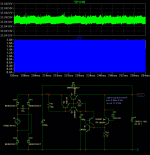
Simulated, ripple is about 1-2 mV at 2A, I haven't tested further than that. At 1A, ripple is about 400uV.
- keantoken
I've been tweaking this design for quite a while now, and want to run it by the DIY community for feedback or suggestions. I have not built it yet, for lack of parts.
This isn't really intended for anything serious, I just started designing to see how well I could do. I figured that in the end I would have a nice lab supply with minimal ripple. Output is around 33VDC but can be changed by using a different zener diode. Adjustable Zener circuits work but not as well as using a single zener.
Rather than a capacitance multiplier, I decided I would go more the route of a specialized (super-sensitive) error amplifier keeping the output voltage steady.
If you want higher current you will need to lower the value of R3.
Q4 and Q6 act as a VERY sensitive feedback pair, which will react when current travels through the Zener diode. The 22 ohm resistor was a 1N34A germanium diode but... they don't exist anymore. The resistor works just as well here I suppose. Operating current through the 22 ohm is at about 20mA, but a .5W resistor is best because failure will likely result in oscillation.
C2 keeps the circuit from oscillating, though it seems from simulation that 100nF is over-conservative.
There is a hitch that I have not been able to work out, which is that the output is most steady after 0.2A, so ideally a class A or AB amp would have a standby current consumption of at least this much. Decreasing input voltage does not affect this. Any suggestions on how to fix this would be helpful.
I know that in the schematic has the input coming from a voltage source and not from a mains transformer. This is because I am lazy, not because I know nothing about safety. In an actual built unit, there would be fuses as well.
Simulated, ripple is about 1-2 mV at 2A, I haven't tested further than that. At 1A, ripple is about 400uV.
- keantoken
Attachments
Hi,
To get a real good feeling for the performance of the circuit, you should also test the ripple as a function of load current frequency. The ripple can be very low at 1kHz, but what at 5kHz, 10kHz, 20kHz?
Also, how does the output voltage change with changing input voltage? And what is the output ripple against the frequency of the input ripple frequency?
Jan Didden
Hi,
It might be OK in simulation but a few things stand out. Q4 what happens when it conducts- it looks like it can pull unlimited base current through Q6. R2 and Q3 ? not sure what you are trying to achieve there") Connecting zeners across potentially "low impedance" points with high current capacity is asking for trouble, any spike will zap it.
Connecting zeners across potentially "low impedance" points with high current capacity is asking for trouble, any spike will zap it.
Keep working on it, do you intend to build it
Edit, I would be nervous with this -- there is the potential for Q2/3/5/7 to put a virtually dead short over the unreg supply through all those B-E junctions. It would take only a brief "spike" to spell disaster. Q4 and Q6 "appear" to form a thyristor. Once Q4 is triggered into conduction Q6 will sustain it's base current whether or not D5 is passing current.
It might be OK in simulation but a few things stand out. Q4 what happens when it conducts- it looks like it can pull unlimited base current through Q6. R2 and Q3 ? not sure what you are trying to achieve there
Connecting zeners across potentially "low impedance" points with high current capacity is asking for trouble, any spike will zap it.Keep working on it, do you intend to build it
Edit, I would be nervous with this -- there is the potential for Q2/3/5/7 to put a virtually dead short over the unreg supply through all those B-E junctions. It would take only a brief "spike" to spell disaster. Q4 and Q6 "appear" to form a thyristor. Once Q4 is triggered into conduction Q6 will sustain it's base current whether or not D5 is passing current.
If Q4 conducts even a small bit, Q6 attempts to turn it hard on. Ideally, this would only happen if the unit started to oscillate since this would pull a lot on Q5s base and turn the whole thing off. However, I see the risk. On a previous version, this would turn on fully in the right conditions and draw around 2A. Those transistors would be history .
It is a very sensitive configuration but it is possible to use it as a super-sensitive voltage sensor in the right conditions. Here, the regulating circuitry will have to react fast enough to cut off that voltage. It's a very precise feedback loop.
Adding a 100k resistor to Q6s emitter seems to work here without degrading performance, although if the pair still turns hard on I think those transistors might be blown. Hmm. I need a protection measure for that...
My initial idea was that Q2 and Q3 would act as a CCS, except that it also drives Q1s base, giving stable voltage across. Now it looks like Q2 and R3 just act a a current divider. I haven't deviated from this, though, since I've found nothing else that works as well. Believe me, I've tried.
Hmm. Looks like we need a fast blow fuse and a sturdy case.
I don't know if thermal switches or fuses would be fast enough, to keep the transistors themselves from acting like fuses.
Any ideas? I think discrete protection circuitry would be best... Hopefully my circuit isn't only good for a toaster. ):
At any rate, here's a AC analysis, using the load as the input, showing the current through the .5 ohm resistor, with the 100k resistor on Q6s base. I found that by using a pass transistor with MUCH less junction capacitance than the 2N3055 (415pF, WHAT!?), this was greatly improved. Unfortunately, that transistor is only rated for 1A, though it will still work in the simulator. Any recommendations for a good pass transistor with low junction capacitance?
- keantoken
.Once Q4 is triggered into conduction Q6 will sustain it's base current whether or not D5 is passing current.
It is a very sensitive configuration but it is possible to use it as a super-sensitive voltage sensor in the right conditions. Here, the regulating circuitry will have to react fast enough to cut off that voltage. It's a very precise feedback loop.
Adding a 100k resistor to Q6s emitter seems to work here without degrading performance, although if the pair still turns hard on I think those transistors might be blown. Hmm. I need a protection measure for that...
My initial idea was that Q2 and Q3 would act as a CCS, except that it also drives Q1s base, giving stable voltage across. Now it looks like Q2 and R3 just act a a current divider. I haven't deviated from this, though, since I've found nothing else that works as well. Believe me, I've tried.
Edit, I would be nervous with this -- there is the potential for Q2/3/5/7 to put a virtually dead short over the unreg supply through all those B-E junctions. It would take only a brief "spike" to spell disaster. Q4 and Q6 "appear" to form a thyristor. Once Q4 is triggered into conduction Q6 will sustain it's base current whether or not D5 is passing current.
Hmm. Looks like we need a fast blow fuse and a sturdy case.
I don't know if thermal switches or fuses would be fast enough, to keep the transistors themselves from acting like fuses.
Any ideas? I think discrete protection circuitry would be best... Hopefully my circuit isn't only good for a toaster. ):
At any rate, here's a AC analysis, using the load as the input, showing the current through the .5 ohm resistor, with the 100k resistor on Q6s base. I found that by using a pass transistor with MUCH less junction capacitance than the 2N3055 (415pF, WHAT!?), this was greatly improved. Unfortunately, that transistor is only rated for 1A, though it will still work in the simulator. Any recommendations for a good pass transistor with low junction capacitance?
- keantoken
Attachments
I remember you.
I'll try not to be such a pain this time. Yes, feedback is fine. If I can't take the heat, that's my problem.
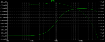
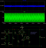
I have been using transient analysis and AC analysis side by side whenever it can help, as much as I know how. I look at the transient at about 10KHz, which is where this PSU operates the worst, and it seems that just plain junction capacitance is what does this. I still can't quite figure out why that bump is always around that area, though. Changing the value of C2 affects ripple greatly. Currently a value of 100p is best, from what it seems. Having C2 at too high a value isn't good, however, because it will trade output stability for input ripple rejection (which isn't what I want).
I've changed the output transistor to a ZTX something, with 7A max current, but the Vceo is 30V and the current Vceo is at max 27V, so I still need a better transistor.
Currently, output changes about 2.2mV from 1A to 2A load.
The image below is an AC analysis with a 1.25-2.25A sine load, probed at the output voltage. The other graph is the load current vs. output voltage at the worst operating frequency, 10KHz.
- keantoken
I'll try not to be such a pain this time. Yes, feedback is fine. If I can't take the heat, that's my problem.
I have been using transient analysis and AC analysis side by side whenever it can help, as much as I know how. I look at the transient at about 10KHz, which is where this PSU operates the worst, and it seems that just plain junction capacitance is what does this. I still can't quite figure out why that bump is always around that area, though. Changing the value of C2 affects ripple greatly. Currently a value of 100p is best, from what it seems. Having C2 at too high a value isn't good, however, because it will trade output stability for input ripple rejection (which isn't what I want).
I've changed the output transistor to a ZTX something, with 7A max current, but the Vceo is 30V and the current Vceo is at max 27V, so I still need a better transistor.
Currently, output changes about 2.2mV from 1A to 2A load.
The image below is an AC analysis with a 1.25-2.25A sine load, probed at the output voltage. The other graph is the load current vs. output voltage at the worst operating frequency, 10KHz.
- keantoken
Attachments
AHA!
Deleting the .5 ohm resistor cures it completely! The error was phase related.
When the load current rises, the output voltage lowers. But this is not because the regulation is faulty, because when the load current lowers, the output voltage is steady.
It seems that removing the .5 ohm resistor keeps the junction capacitance from becoming much of a problem.
Now the ripple at 10KHz is about 10mV.
It seems more prone to oscillate now, though, but it looks like 100p is enough to keep it under control.
- keantoken
Attachments
Hi,
I will keep looking in . I have the greatest admiration for you guys that design on the simulator ( something I have never got into ) . Ultimately your going to have to actually build it and do some real measurements. Looking at your latest circuit, have you added any rail capacitance to the output and local decoupling for R.F. stability. Does R6 need to be so low ? I can't just grasp the function of Q6. ( I can see what you are trying to do but the whole error amp looks to convoluted ).
Quite a good test (to do for real) is to place a power transistor (HEXFET is ideal) but any high gain high speed power Bjt will do across the output with a resistor that will draw say 2 amps from the supply. Drive the base or gate with a squarewave and look at the actual ripple and rail fluctuations. You can drive it from DC up to say 40 or 50 Khz. Very revealing.
I will keep looking in
. I have the greatest admiration for you guys that design on the simulator ( something I have never got into ) . Ultimately your going to have to actually build it and do some real measurements. Looking at your latest circuit, have you added any rail capacitance to the output and local decoupling for R.F. stability. Does R6 need to be so low ? I can't just grasp the function of Q6. ( I can see what you are trying to do but the whole error amp looks to convoluted ).Quite a good test (to do for real) is to place a power transistor (HEXFET is ideal) but any high gain high speed power Bjt will do across the output with a resistor that will draw say 2 amps from the supply. Drive the base or gate with a squarewave and look at the actual ripple and rail fluctuations. You can drive it from DC up to say 40 or 50 Khz. Very revealing.
I only expect to add rail capacitance to the output when I actually try and connect it to something. As for now, I want to get it as good as possible in a linear fashion, with as little as possible AC components.
And what exactly does 'local decoupling' mean? I probably know what it is but the jargon escapes me.
R6 is quite low but I found this was the optimal value by playing around in the sim. Curious that it also matches about the resistance of the 1N34A diode in the same situation...
Documentation on the Q4/Q6 pair can be found here although not in the way I use it. I find it weird that I have not seen a link to this site on DIYAudio once... Maybe everyone else knows something I don't?
I will remember this one. Sounds like it's liable to make something explode though. I can just hear some cheap electrolytic start fizzing shortly before popping and smelling very very bad. I would actually prefer to be more gentle with my circuits! Something like that really scares me... But I guess I need some more experience to really know what to expect...
- keantoken
And what exactly does 'local decoupling' mean? I probably know what it is but the jargon escapes me.
R6 is quite low but I found this was the optimal value by playing around in the sim. Curious that it also matches about the resistance of the 1N34A diode in the same situation...
Documentation on the Q4/Q6 pair can be found here although not in the way I use it. I find it weird that I have not seen a link to this site on DIYAudio once... Maybe everyone else knows something I don't?
Quite a good test (to do for real) is to place a power transistor (HEXFET is ideal) but any high gain high speed power Bjt will do across the output with a resistor that will draw say 2 amps from the supply. Drive the base or gate with a squarewave and look at the actual ripple and rail fluctuations. You can drive it from DC up to say 40 or 50 Khz. Very revealing.
I will remember this one. Sounds like it's liable to make something explode though. I can just hear some cheap electrolytic start fizzing shortly before popping and smelling very very bad. I would actually prefer to be more gentle with my circuits! Something like that really scares me... But I guess I need some more experience to really know what to expect...
- keantoken
Hi,
"Local Decoupling" The output impedance of any series reg like this will increase with frequency. It just means adding something like a 0.1 mfd across the output to maintain a low impedance at HF. I still can not see what Q6 does other than form a thyristor as I mentioned earlier. As you had it in the earlier circuit it formed a "crowbar" across the rail but now with a 100 k in the emmiter --- what is it's function ? Transistors connected like this used to be available as type BRY39 and BR101 used for triggering of thryistor based PSU in old tellys etc.
"Local Decoupling" The output impedance of any series reg like this will increase with frequency. It just means adding something like a 0.1 mfd across the output to maintain a low impedance at HF. I still can not see what Q6 does other than form a thyristor as I mentioned earlier. As you had it in the earlier circuit it formed a "crowbar" across the rail but now with a 100 k in the emmiter --- what is it's function ? Transistors connected like this used to be available as type BRY39 and BR101 used for triggering of thryistor based PSU in old tellys etc.
NEATO!
Alright, thanks.
You know what, you're exactly right... I deleted Q6 and got better results.
I then ran through several different versions of the circuit. This is pretty amazing. Hopefully I haven't fallen into a simulator ditch here, because this is very nice.
Naturally, the more components you take out, the smoother the remaining devices work.
I tried replacing R3 with a CCS, to help input ripple rejection... I failed horribly, and got a better circuit from the experience!.
I deleted the CFP pair, and just hooked Q2 and R3 up to a new PUT pair, and whoah...
With the new circuit (attached) if I put the value of R1 below 30k, the ripple rejection OVERCOMPENSATES. Yes. The output voltage is actually an inverted version of the input...
But the higher I make R1, the less output ripple rejection...
So if R1 is below 30k, you trade output rejection for input rejection. If it is above 30k, you trade input rejection for output rejection.
Currently the circuit is in a very controlled state... By adjusting R1, you can have a little 120Hz ripple but virtually no output ripple, or you can have virtually no 120Hz ripple, but a little output ripple.
This simple circuitry is effective! In the simulator, at least. I really do need to build this thing. I don't have a good pass transistor though... Urgh... Must... Build...
Hmm. Would a 2SC3996 work as the pass transistor here?
- keantoken
Alright, thanks.
I still can not see what Q6 does other than form a thyristor as I mentioned earlier.
You know what, you're exactly right... I deleted Q6 and got better results.
I then ran through several different versions of the circuit. This is pretty amazing. Hopefully I haven't fallen into a simulator ditch here, because this is very nice.
Naturally, the more components you take out, the smoother the remaining devices work.
I tried replacing R3 with a CCS, to help input ripple rejection... I failed horribly, and got a better circuit from the experience!.
I deleted the CFP pair, and just hooked Q2 and R3 up to a new PUT pair, and whoah...
With the new circuit (attached) if I put the value of R1 below 30k, the ripple rejection OVERCOMPENSATES. Yes. The output voltage is actually an inverted version of the input...
But the higher I make R1, the less output ripple rejection...
So if R1 is below 30k, you trade output rejection for input rejection. If it is above 30k, you trade input rejection for output rejection.
Currently the circuit is in a very controlled state... By adjusting R1, you can have a little 120Hz ripple but virtually no output ripple, or you can have virtually no 120Hz ripple, but a little output ripple.
This simple circuitry is effective! In the simulator, at least. I really do need to build this thing. I don't have a good pass transistor though... Urgh... Must... Build...
Hmm. Would a 2SC3996 work as the pass transistor here?
- keantoken
Attachments
Hi,
It's looking more conventional now. You are trying to regulate the voltage by having a transistor shunt base current away from the two main devices, Q1 and Q2 when the output exceeds a voltage determined by the zener.
As you have it now try removing Q5 altogether.
What does Q3/R2 do. It will work without these I think. Connect the collector of Q7 to the base of Q2.
Have you tried rearranging it bit. Remove the bits as above. Replace the zener and R5 with a pre set pot say 10k with the wiper to the base of Q7. Add a zener in series with the emmiter of Q7 to ground around say 5.6 volt. This will form a proper error amp, and you can adjust the output voltage with the pot. Also value of R1 at 30k seems high -- not enough base current under high loads. You can always add current limiting in afterwards.
With the simulator can you add the MOSFET or Bjt I mentioned earlier and see the effect on the output.
Hi,
It's looking more conventional now. You are trying to regulate the voltage by having a transistor shunt base current away from the two main devices, Q1 and Q2 when the output exceeds a voltage determined by the zener.
As you have it now try removing Q5 altogether.
Q5 is the trump card of the entire circuit... Q7 and Q5 form the error correction circuitry, and very effectively, at that.
What does Q3/R2 do. It will work without these I think. Connect the collector of Q7 to the base of Q2.
Have you tried rearranging it bit. Remove the bits as above. Replace the zener and R5 with a pre set pot say 10k with the wiper to the base of Q7. Add a zener in series with the emmiter of Q7 to ground around say 5.6 volt. This will form a proper error amp, and you can adjust the output voltage with the pot.
The fact is that we don't really know what EXACTLY Q3 and R2 do, but what they do, they do GOOD. Nothing else I've ever tried has beat this.
The problem with adding a POT as you said, is that the resistance will leech the high-sensitivity of the Q7/Q5 pair, along with the Zener, which effectively destroys the circuit's ability to regulate voltage as good as it does. This is the only reason I haven't added a way to vary output voltage easily.
This will form a proper error amp, and you can adjust the output voltage with the pot. Also value of R1 at 30k seems high -- not enough base current under high loads. You can always add current limiting in afterwards.
With the simulator can you add the MOSFET or Bjt I mentioned earlier and see the effect on the output.
At least as far as 2A, R1 is fine. The most I'll be driving with this will probably be Symasym, a 120W amp. What is really supplying the pass transistor with its base current is Q2. This forms a darlington pair with plenty of gain, so I don't really need a very low value to get high currents out of this circuit.
The problem is, I am not trying to make a 'proper' PSU. I'm trying something different because the circuit you're turning this into is about 100X worse than my original, when I simulate it. (I am not angry, I'm just trying to be honest).
After making these changes that you suggest, I really have nothing different from the conventional voltage regulator skeleton. It may be the underlying principle, but alone it doesn't do anywhere near as good as if I leave all the modifications on.
I have looked at and understood the design of the regulator you suggested I turn this into, which is why I'm trying to make something better.
I'm not angry with you, mooly. I'm just not sure you understand what I'm trying to do here.
I guess your alternative is more convenient, but what I'm going for here is accuracy. I can live with inconvenience if I get enough out of it.
Although, I haven't tried substituting the Zener for the adjustable zener circuit below...
http://www.tubecad.com/june2000/page3.html
I could use a POT in this and it would probably work better for this circuit than what you suggested. I still want to see what kind of performance I can crank out of this first, though.
EDIT: I have to go to sleep now... I've stayed up for about two days and a half without sleep. I really don't understand how. My brain isn't any slower (that I've noticed) than when I wake up. I didn't feel tired, so I just kept going... For two and a half days.
But at any rate, even if my mind is not feeling tired, my body is. I must rest my body...
- keantoken
I am definitely going to build this thing.
But I don't have parts... I think my 2SC3996 will work (a high-voltage CRT deflection transistor from and old computer monitor).
I have a few 2N5087s, which are apparently good for PSUs, because of their low junction capacitance. But apart from that I don't have any other transistors as suitable as them, except for HF transistors from the old computer monitor, and using those things for this I think is asking for HF oscillation.
I don't have a Zener diode...
This is naturally a not humongous design because I am trying to design it so that I actually can build it, so this is a plus.
So yes, I will build the darn thing.
I just don't know when I'll be able to. ):
I can probably change the Zener to different voltages and it'll work just as well.
At any rate, back to the circuit.
I know that Q3 and R2 to regulate the Vbe of Q2, as this was what I designed it to do. R3 is just low enough to put a good .6V Vbe for Q3. Higher resistors cause worse regulation, so it looks like this is the sweet spot. The base current for Q3 is about 10-15uA, which I find is the place where most transistors will operate their best for lowest input distortion. So I don't think the Q3/R2 occurance is a flaw.
I simulated with a 1N750 4.7V Zener, at the same currents, and the regulation is still quite good! So I think this circuit will work for any voltage, as long as the devices are properly selected and R1 is say a 50K trimpot.
I will try simulating with the high-power transistor on the output as you suggest, and I will also try using the adjustable zener circuit and see what it does to the quality of output.
- keantoken
But I don't have parts... I think my 2SC3996 will work (a high-voltage CRT deflection transistor from and old computer monitor
).I have a few 2N5087s, which are apparently good for PSUs, because of their low junction capacitance. But apart from that I don't have any other transistors as suitable as them, except for HF transistors from the old computer monitor, and using those things for this I think is asking for HF oscillation.
I don't have a Zener diode...
This is naturally a not humongous design because I am trying to design it so that I actually can build it, so this is a plus.
So yes, I will build the darn thing.
I just don't know when I'll be able to. ):
I can probably change the Zener to different voltages and it'll work just as well.
At any rate, back to the circuit.
I know that Q3 and R2 to regulate the Vbe of Q2, as this was what I designed it to do. R3 is just low enough to put a good .6V Vbe for Q3. Higher resistors cause worse regulation, so it looks like this is the sweet spot. The base current for Q3 is about 10-15uA, which I find is the place where most transistors will operate their best for lowest input distortion. So I don't think the Q3/R2 occurance is a flaw.
I simulated with a 1N750 4.7V Zener, at the same currents, and the regulation is still quite good! So I think this circuit will work for any voltage, as long as the devices are properly selected and R1 is say a 50K trimpot.
I will try simulating with the high-power transistor on the output as you suggest, and I will also try using the adjustable zener circuit and see what it does to the quality of output.
- keantoken
Attachments
Connecting zeners across potentially "low impedance" points with high current capacity is asking for trouble, any spike will zap it.
I believe I have found a solution
.This solution does not only help with that one problem, however.
The solution is to place transistor Q4, and put the Zener across its B-C junction.
This makes the Zener super-sensitive, and puts it closer to its ideal breakover voltage. With this arrangement, a brief voltage spike would quickly be shorted by Q4, and then by the pass transistor. Because of the low resistance of R3, Q7 is also not as susceptible to voltage spikes.
Because of this added sensitivity, Q7 now draws less current, meaning more headroom is left for the pass transistor, meaning that we can further lower R1.
The Zener has significant junction capacitance, 220pF!. However, the 2N5089 only has about 4pF, and thus, even when HF ripple is enough to defeat the zener diode, this will still modulate Q4s current, and it will still regulate.
Also, I have found a better place for C2, the capacitor required to keep the circuit from oscillating. It's in a much more sensitive area of the circuit, which means it can be lower and have just as much effect as the old position.
With these improvements, the circuit now simulates with 200uV of line ripple at 10Khz.
Attachments
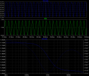
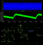
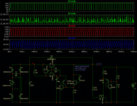
Mooly, your test circuit suggestion is a VERY, VERY rough test! I now understand why it is as revealing as it is...
If the correction circuits aren't as fast as the risetime of the squarewave, you either get voltage dip, or a voltage spike, depending on how your circuit works. Thankfully, we get a voltage drop with this one.
However, the spike is apparently enough to cause the circuit to go into oscillation... I always know when my circuit oscillates because the simulator get reaaally slooooooow.
The square wave source is my own circuit, stemming from the PUT oscillator found on the webpage I mentioned earlier. It is a quick & Crappy (TM) solution, but it is very convenient when you want superfast switching times, at high currents. The circuit oscillates using the miller capacitance of the MOSFET.
At any rate, the result. The circuit operates as I expected it to, except for the oscillation...
The pattern shown exhibits a beat frequency in the decay rate of the oscillation, and I'm willing to bet it has something to do with the input voltage ripple. See how the frequency of the input ripple and the frequency of the load are so similar? The beat frequency of those two shows up in the output, because it has something to do with the circuit's ability to oscillate.
This means that either
1: At lower input voltages the circuit can facilitate more oscillation (the longer decay rate of the oscillation observed). Or,
2: The rate of change of the input ripple, in addition to the output pulses, causes stronger oscillation start, which causes the oscillation to last longer, e.g. longer decay rate.
Based on the observations, #1 appears to be the most likely...
So, I will next attempt to help the oscillation without altering C2, which would degrade performance. My first act will be to increase supply voltage, the most obvious considering the nature of cause #1...
I thank you for your test circuit, Mooly. It is very revealing even on the simulator, and it is a precious gem of knowledge... A lot can be learned and enhanced by using this circuit...
- keantoken
Attachments
Interesting to see it as a simulation. It is a tough test, I agree.
I know and respect you want to try things out for yourself, I will just say look at Q5 Q7 and C2. Isn't this essentially (not quite I know but all the ingredients are there) the same as the PUT oscillator.
Regards Karl
I know and respect you want to try things out for yourself, I will just say look at Q5 Q7 and C2. Isn't this essentially (not quite I know but all the ingredients are there) the same as the PUT oscillator.
Regards Karl
EDIT: Oh, I didn't see you post!. I hadn't seen it that way... I'm glad you pointed that out. Yes, I now understand the circuit better. If C2 is too high, the circuit will definitely oscillate! The reason it doesn't at stable voltages is mostly because of R3... R3 lowers the gain of the PUT pair, so that it cannot react fast enough to cause oscillation. So if C2 is too low to absorb the spike if the PUT suddenly turns on, the circuit will oscillate. It will also oscillate if the capacitor is large enough to delay the feedback signal too much. It would have to be fairly large for the circuit to oscillate in this way (with the modifications below), however...
BTW, If this circuit works in real life as well as it does in the sim, how good is it compared to most PSUs posted here?
actual post:
Sorry for double post, but there's a 1-image per-post limit, apparently.
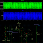
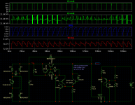
If you look at the above graph and this one, you'll notice the weird jagged things on the output trace. I'm not sure but I believe these are artefacts caused by simulation errors, and they happen when the sim's ability to compute is limited by the 32-bit maximum accuracy of digital processing. Apparently this test is so intensive the results are difficult for the sim to calculate... At any rate this used to happen a lot when I first got the simulator and was making horrendously flawed circuits... It used to confuse a lot because I didn't know what was happening.
At any rate, the problem with oscillation was fixed by increasing supply to 70V. So I narrowly avoided having to increase C2, which would degrade performance at high frequencies.
I will try and take pictures of the devices I will try to build it with, as I really do want to build it, even more so since I did a complete recal of my oscilloscope.
Unfortunately, I may not be able to... Is there anyone else who would be willing to build it?
- keantoken
BTW, If this circuit works in real life as well as it does in the sim, how good is it compared to most PSUs posted here?
actual post:
Sorry for double post, but there's a 1-image per-post limit, apparently.
If you look at the above graph and this one, you'll notice the weird jagged things on the output trace. I'm not sure but I believe these are artefacts caused by simulation errors, and they happen when the sim's ability to compute is limited by the 32-bit maximum accuracy of digital processing. Apparently this test is so intensive the results are difficult for the sim to calculate... At any rate this used to happen a lot when I first got the simulator and was making horrendously flawed circuits... It used to confuse a lot because I didn't know what was happening.
At any rate, the problem with oscillation was fixed by increasing supply to 70V. So I narrowly avoided having to increase C2, which would degrade performance at high frequencies.
I will try and take pictures of the devices I will try to build it with, as I really do want to build it, even more so since I did a complete recal of my oscilloscope.
Unfortunately, I may not be able to... Is there anyone else who would be willing to build it?
- keantoken
Attachments
- Status
- This old topic is closed. If you want to reopen this topic, contact a moderator using the "Report Post" button.
- Home
- Amplifiers
- Power Supplies
- Linear Pass transistor regulator - my design