Nonsense, the problem is you, and your poor understanding of basic electronics, that would not be such a problem if you would listen to what you are told to do. I repeatedly sayd you have misswind the power transformer but you completely ignored that, thus you failed...After doing many works on this SMPS and consulting with professionals, it turned out that this design has many problems and WILL NOT work. Even if it was a working circuit, it would not be a suitable power supply for Audio amplifiers.
So I recommend you NOT TO TRY THIS.
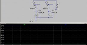
The switching supply presented in the schematic really does work, and is usable in audio ( many have ). Have a look in the schematic at the power transformer, it is ETD59 and it has 12 turns on the primary side, and 2x6 turns on the output, thus the turn ratio is 12/6, or 2. At 150V on the primary side, it gives 150/2 on the output, that's 75V, the outputs are marked as 2x70V, so already sounds ok because the power transformer's pulses are greater than the desired output voltage, that is normal, in fact it's mandatory. If we calculate the regulated voltage with that feedback loop as i have explained earlyer, we find about 71V wich is fairly close to the numbers, so the schematic really is ok, but you are the one that ignores basic rulles.
I can help with all the calculations needed but you have to do exactly what you are sayd, i need to know every single modification you have made to the original schematic, i also need to know exactly what power transformer you use ( size and core mix ), and last but not the least what output voltages you need and at what power. Only with carefull adaptation and calculation you cand make work a modifyed SMPS.
Good luck.
Last edited:
(But 0th step is getting an oscilloscope and -1th step is understanding basics of electronics.)
I don't see serious problems. Feedback is not very good indeed, but placing a resistor into the COMP pin can help.
- Zener(s) current would be very likely much lower than needed (remedy: shunt optocoupler LED with a resistor)
- Compensation network looks weird. There is a cap from COMP output to the ground while SG3525 feedback amp isn't a transconductance one (why not use plain Type II compensation instead?)
Chances are the regulation and stability depend on component selection.
collecting parts
Hi,
I discover this thread, and I tought yes, this is a good
possibility, not only the circuit, but here are people
with understanding and clear statements.
I will make a smps fore a poweramp. +/- 50 V and
100-125 W power.
So I start searching parts, I see cheep and more expensive parts, the mosfet, the transformer, the
sg 3525, the difference is the extension in the name,
and the price.
Can I buy what I will?
Is it posible to use a toroid coil?
I know that I need a coil whit a gape.
The ETD59 is availeble whit a squar or a round leg.?
I have not found a BOM
Thank you.
- Zener(s) current would be very likely much lower than needed
Why??? If it is low, then what makes duty cycle too low?
(remedy: shunt optocoupler LED with a resistor)
Why? To make useful current even lower?
- Compensation network looks weird. There is a cap from COMP output to the ground while SG3525 feedback amp isn't a transconductance one
Actually it is.
Due to CTR of the opto and opto transistor load the current thru opto's LED.Why??? If it is low, then what makes duty cycle too low?
To increase current flowing through Zeners to ensure we get desired 36v drop. Check BZX85C36 datasheet, specified 36v is at 8 mA.Why? To make useful current even lower?
Last edited:
SG3525 op-amp is a conventional operational [voltage] amplifier. It's wired w/o negative feedback, thus having large open loop gain it works more like a comparator, not an error amplifier. The cap at the comp pin to ground doesn't help much unless OPA output short circuit protection kicks in (do not remember if there is one in 3525 PWM).Actually it is.
All that doesn't help with taming the NFB loop.
Last edited:
Transconductance is specified.
http://www.st.com/web/en/resource/technical/document/datasheet/CD00000958.pdf
Page 3: "DC Transconduct. 30 KΩ ≤ RL ≤ 1 MΩ
Tj = 25 °C
1.1 1.5 1.1 1.5 ms"
Or you can analyse the schematic (figure 5). (Current output.)
And here the zener current is somewhere around 5 mA. Do you really think Zener voltage can be less then 2 V at this current? Can it be a Zener then? Absolutely no. It can be either shorted, or reversed.
Or something else is damaged, completely different from specification, etc... But the most probable reason of the experienced behaviour is reversed zener.
Zener voltage depends on current very moderately. This is exactly why we use them. For example 36V at 8 mA, 35.7 V at 1 mA, and about 35V at 0.1 mA.
http://www.st.com/web/en/resource/technical/document/datasheet/CD00000958.pdf
Page 3: "DC Transconduct. 30 KΩ ≤ RL ≤ 1 MΩ
Tj = 25 °C
1.1 1.5 1.1 1.5 ms"
Or you can analyse the schematic (figure 5). (Current output.)
Oh my god! Do you regularly change the causality order? Opto transistor doest'n have any direct effect on LEDs current. It works only indirectly, through SG3525, but with the other polarity: low current would make high duty cycle, high output voltage, what would make zener current high enough. This is how negative feedback works. What we see now is a contradiction. Negative feedback is ensured by topology, so in this circuit your initial assumption (nothing is wrong only zener current is low) must be false. Logic.Due to CTR of the opto and opto transistor load the current thru opto's LED.
To increase current flowing through Zeners to ensure we get desired 36v drop. Check BZX85C36 datasheet, specified 36v is at 8 mA.
And here the zener current is somewhere around 5 mA. Do you really think Zener voltage can be less then 2 V at this current? Can it be a Zener then? Absolutely no. It can be either shorted, or reversed.
Or something else is damaged, completely different from specification, etc... But the most probable reason of the experienced behaviour is reversed zener.
Zener voltage depends on current very moderately. This is exactly why we use them. For example 36V at 8 mA, 35.7 V at 1 mA, and about 35V at 0.1 mA.
Sigh. Unfortunately transoconductance isn't specified for load less than 30k and also it's not specified for 3525 made by fairchild, onsemi, microsemi). Probably because the error amp isn't a transconductance oneTransconductance is specified.
http://www.st.com/web/en/resource/technical/document/datasheet/CD00000958.pdf
Page 3: "DC Transconduct. 30 KΩ ≤ RL ≤ 1 MΩ
Tj = 25 °C
1.1 1.5 1.1 1.5 ms"
Or you can analyse the schematic (figure 5). (Current output.)
") and it's not advised to use it like that.
and it's not advised to use it like that.Shunting opto's LED will increase Zener current. That happens due to negative feedback *loop*. You can easily analyze the feedback loop going "backwards" assuming SMPS is in steady state.Oh my god! Do you regularly change the causality order? Opto transistor doest'n have any direct effect on LEDs current. It works only indirectly, through SG3525, but with the other polarity: low current would make high duty cycle, high output voltage, what would make zener current high enough. This is how negative feedback works. What we see now is a contradiction. Negative feedback is ensured by topology, so in this circuit your initial assumption (nothing is wrong only zener current is low) must be false. Logic.
I'm attaching a pic to illustrate that. In steady state Vbe would be ca. 0.65v, assuming the base current is much less than zener current we can easily calculate zener current for both cases: it would ba ca. 1mA and 0.5 mA.
It works just like that with the opto's LED & Zener current.
A bit offtopic but people often "change casuality order", check it out: https://en.wikipedia.org/wiki/Backward_induction https://en.wikipedia.org/wiki/Backward_chaining https://en.wikipedia.org/wiki/Backward_induction etc
I'm not sure we are on the same page. What does "voltage can be less then 2 V at this current" mean?And here the zener current is somewhere around 5 mA. Do you really think Zener voltage can be less then 2 V at this current? Can it be a Zener then? Absolutely no. It can be either shorted, or reversed.
Or something else is damaged, completely different from specification, etc... But the most probable reason of the experienced behaviour is reversed zener.
Your generalization is false. Please google "zener knee voltage" "zener knee current" and/or check this link: Lecture 8Zener voltage depends on current very moderately. This is exactly why we use them. For example 36V at 8 mA, 35.7 V at 1 mA, and about 35V at 0.1 mA.
I don't see any data on that in BZX85C series zeners datasheet and I do not want to guess (we are after reliable design, right?) however I see test current is specified (8 mA). Thus the way to go is to ensure the current flowing through the zener is more than that (but still within thermal limits).
Attachments
Sigh. Unfortunately transoconductance isn't specified for load less than 30k and also it's not specified for 3525 made by fairchild, onsemi, microsemi). Probably because the error amp isn't a transconductance one
Look at the test circuit on datasheets! All of them specifies it with 10 nF on output of error amp.
Shunting opto's LED will increase Zener current.
In a properly working circuit. Is this the situation? No. What we know: output voltage was veeery low. Can there be zener current? No way!
That happens due to negative feedback *loop*. You can easily analyze the feedback loop going "backwards" assuming SMPS is in steady state.
I did it first with the known schematic, and based on that I told no serious problem with the design. But the built circuit didn't work. So it must be different. So you can't analise it, because you don't know it, you don't know the difference. But I proposed a reason with a single error that can explain the experienced problem. Did you understand it?
I'm attaching a pic to illustrate that. In steady state Vbe would be ca. 0.65v, assuming the base current is much less than zener current we can easily calculate zener current for both cases: it would ba ca. 1mA and 0.5 mA.
This has no relevance to zener. Please note I perfectly know how feedback work. But you talked about zeners. Did you measure zener voltages in your simulation? Do they differ significantly? Are they much lower then specified? I bet not. Then your remedy is not working. The diagnosis was already false. You should have calculated opto current, as I did.
It works just like that with the opto's LED & Zener current.
Thanks but I don't need teaching. I know how should have worked, but here it didn't work, what is the problem itself.
A bit offtopic but people often "change casuality order", check it out: https://en.wikipedia.org/wiki/Backward_induction https://en.wikipedia.org/wiki/Backward_chaining https://en.wikipedia.org/wiki/Backward_induction etc
It exists but you didn't use it in the right way, right case. And backward induction is not changing casuality order.
I'm not sure we are on the same page. What does "voltage can be less then 2 V at this current" mean?
There is not much posts about this. Originally here (on previous page):
http://www.diyaudio.com/forums/power-supplies/125269-50-v-smps-10.html#post4335298
But you replied to my post. It was also there in the quote. Haven't you read it? It's a pity. We could have been avoid a painful debate.
Your generalization is false.
In what way??? Proove!
Please google "zener knee voltage" "zener knee current" and/or check this link: Lecture 8
I know zeners better than this. But nothing is contradictional here to my statement.
I don't see any data on that in BZX85C series zeners datasheet and I do not want to guess (we are after reliable design, right?)
No. My reason was debugging a wrongly built one. No designing here.
however I see test current is specified (8 mA). Thus the way to go is to ensure the current flowing through the zener is more than that (but still within thermal limits).
I designed and measured enough zener-stabilised SMPS to tell you for sure that here zener current is not small, but quite high, and not limited (which can possibly make it go to a dead short). 1 mA is perfectly enough for a 36V zener. At 10 uA it's already near the nominal voltage. If you don't know zeners enough: measure! I did. No need for lecture.
Zeners over 5V are quite steep. Low voltage ones are not that good. 2V7 is very bad.
If a current flowing through Zener is less than the knee current you wont get "stable" voltage drop (please learn how to read Current-Voltage curves, see https://en.wikipedia.org/wiki/Current–voltage_characteristic )In what way??? Proove!
I know zeners better than this. But nothing is contradictional here to my statement.
I'm not going to "Proove" anything to a person who can't read I/V curves and have issues with NFB loop analysis. I already spent too much time explaining very basic stuff (with no luck).
If a current flowing through Zener is less than the knee current you wont get "stable" voltage drop
And what do you think knee current is? 10 uA? 100 uA? Over 4 mA? Have you ever measured one? I did, many times. Do you think ignorance overrides experience? Have you ever checked leakage current specification of zeners?
(please learn how to read Current-Voltage curves, see https://en.wikipedia.org/wiki/Current–voltage_characteristic )
This is an unreasonable, irrelevant personal attack. Stop it now!
I'm not going to "Proove" anything to a person who can't read I/V curves
You have no right and you have no ability to judge my skills. And you have nothing to base it on. You haven't linked any real I/V curves, only some intentionally distorted simplifications. You are misdirected (...by yourself actually).
If you think I lie, read it from ONsemi:
http://www.onsemi.com/pub_link/Collateral/HBD854-D.PDF Figure4. You can clearly see that zener voltage is at least as stable at 0.1 mA as at 10 mA, or much stable depending on temperature changes.

Yes, you really did and shouldn't. Educate yourself! And read before reply!I already spent too much time explaining very basic stuff (with no luck).
Hi Mahmood,hi
this is the pcb layout of my newly project in two part .
1st main board is power section & 2sd is PWM section
of course i used a few SMD components in PWM pcb
EDT 44
pri 36 [turn]
sec 4 [turn] " center tab "
pri wire size : 4*26 (AWG)
sec wire size : 33*26(AWG)
part one bottom side :
Please, I am interested by the final schematic if U could send it to my mail box christ_nicobis@yahoo.fr.
Thanks
http://www.diyaudio.com/forums/members/mahmood.html
Thanks for a very useful link, if a bit long and somewhat complicated.read it from ONsemi:
http://www.onsemi.com/pub_link/Collateral/HBD854-D.PDF .......
Thanks for a very useful link, if a bit long and somewhat complicated.
You're welcome!
- Status
- This old topic is closed. If you want to reopen this topic, contact a moderator using the "Report Post" button.
- Home
- Amplifiers
- Power Supplies
- -/+ 50 v SMPS